|
|
|
Jo's Radio Collection
Introduction
First of all, let me introduce myself. I am Jo Bleijlevens and
live in the most southern part of Holland. My passion for old
radios is obvious if you consider my electro-technical
education that is primarily focused on electronics. Apart from
that I have also good knowledge of fine mechanical
engineering.
As a little boy of 6 years old, I demolished just everything that was
dumped in the wastebasket in order to satisfy my
curiosity how the "thing" operated and how it had been
assembled. Even when I was at an elderly age, I completely
demolished a very old Philips radio model 2531 and loudspeaker
model 2019. I loved that red horseshoe shaped magnet that was
inside the loudspeaker. It was really attractive.
In this mode of operation, quite some old radios and
television sets have met my sledgehammer.
It has been a strange experience that, at a more mature age, I
became remorseful with respect to this nostalgic demolishing behavior.
The trigger for this remorse occurred when I saw on the
Internet various pictures of old radios that did look very
familiar to me.
From that moment on I furiously started collecting old radios
because I would like to see the vintage glowing of the
electron tubes again and to hear that nostalgic sound from the
loudspeaker. In 2006, I became a member of the NVHR which is
the Dutch Society for the History of the Radio inaugurated in
1977. That membership gave me the
opportunity to visit exhibitions where you can exchange
and/or buy radios and all kind of spare parts for radios.
At this moment my radio collection merely consist of Philips
radios that have been thoroughly renovated in the course of
the past years.
This renovation project resulted in an acceptable quality of
sound of all radios. For achieving the success of this
renovation project, I have to thank Jan Post from Australia and
Ben Dijkman and Corrien Maas from Holland who all delivered the required
components to make this radio collection a complete one.
Corrien Maas delivered the beautiful hand-woven radio fabric that
gives each radio its own particular appearance. I also have
to express my thanks and gratitude to my old Medtronic
colleague Volkert Zeijlemaker who donated a so called home
build Schaaper radio.
On a morning, he saw this particular radio laying on his neighbor's sidewalk.
Obviously, the radio was intended to be
collected by the garbage men later that day.
He rapidly took it away and asked me whether I was interested in
it. My obvious response was yes and I said that I had certainly
interest in that piece of junk. I took it home with the intention to
demolish it again for having some spare parts at hand. However, before
doing so, I desperately wanted to know what the device really was
meant to be since I had a slight hunch that it was not just a simple home
built hobby wireless receiver.
As I said earlier, I became a member of the NVHR and as a member of
the club you
communicate a lot with your fellow NVHR members.
So, one time I sent an e-mail to NVHR member Wim Stuiver to ask him
where I could get an FM tuner for a Philips radio model BX410A. In the same e-mail
I asked him whether he happened to have some information about the radio shown on the attached
picture in the e-mail.
He told me in a reply e-mail that I happened to be the lucky owner of a so-called Erik Schaaper radio that was a home built radio dated from back
in 1931-1934. In that time frame Erik Schaaper had a small factory in
Utrecht where he designed and manufactured parts for home build radio
sets. One had to buy all the single components and the schematic in order
to assemble the wireless receiver at home.
To complete this introduction, I will give you a
small summary of what will be discussed in the following chapters. In the first chapter, I will give a summary of my radio collection
followed by a chapter on useful hints that may help you in the renovation of
old radios in order to regain that nostalgic sound again out of the device.
In the third chapter I will
try to present an historical overview of how the
very first electron tube evolved into the today well- known integrated
circuit chip that contains millions of single transistors which are
actually the successors of the vintage electron tubes.
The fourth chapter depicts the development of electronic
components and their packaging
throughout the years.
Chapter 1 Radio collection
1.1 Philips Radios Click on the pictures to
show them enlarged in a new window
 |
 |
|
 |
 |
|
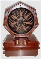
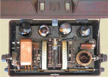
2531 with loudspeaker model 2019
Manufactured in 1932
Tubes: E442, E424, C443, 506
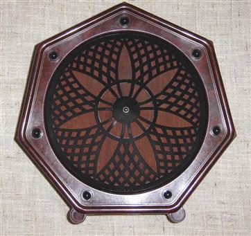
|
2019
Speaker |
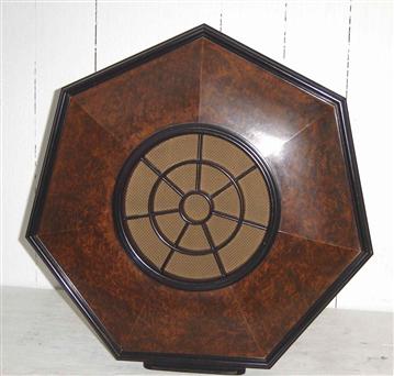
2115
Speaker |
 |
 |
|
 |
 |
|
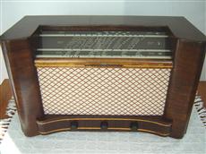
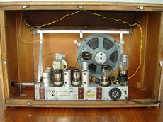
836A Manufactured in
1934
Tubes: E455, E462, E499, E443H, 1823
|
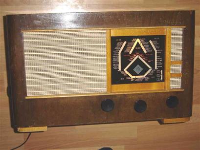
V6A Manufactured in 1937
Tubes: AK2, AF3, ABC1, AL4, AZ1
|
 |
 |
|
890A Manufactured in 1937
Tubes:
AF3, AK2, ABC1, ABC1, AL4, AL4,
AM1,
AZ1, 1823
|
 |
|
 |
|
890A Station-scale
|
890A
Tuning indicator (Magic eye)
|
 |
 |
|
650A Manufactured in
1938
Tubes: EK2, EF8, EF9, EBL1, EM1, AZ1
|
 |
 |
|
 |
 |
|
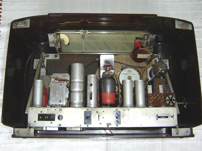
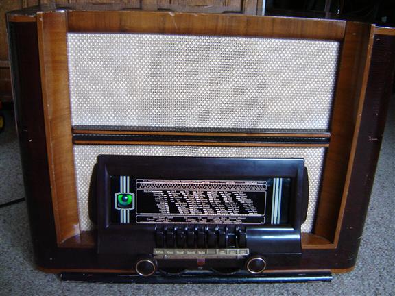
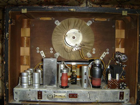
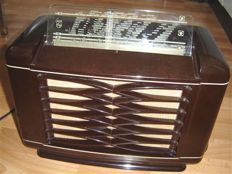
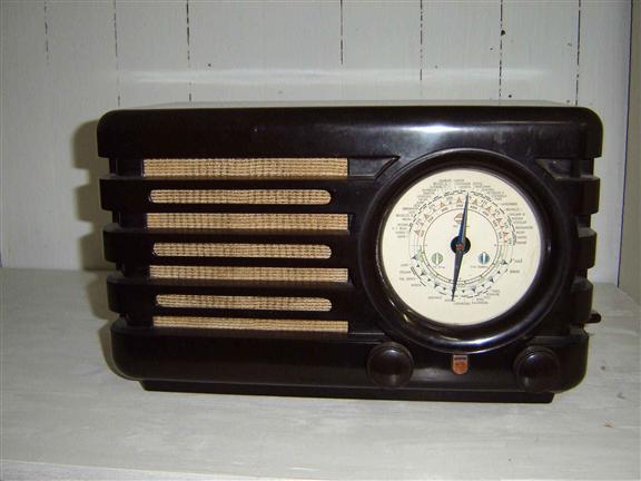
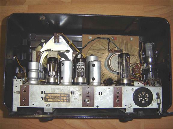
905X Manufactured in 1940
Tubes: EF8, ECH3, EF9, EFM1, EBL1, AZ1 |
BX462A Manufactured in 1946
Tubes: ECH21, ECH21, EBL21, AZ1 |
 |
 |
|
 |
 |
|
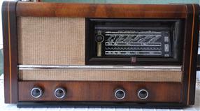
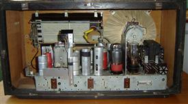
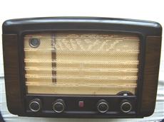
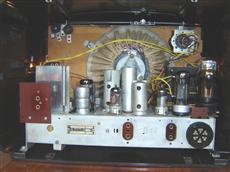
BX360A Manufactured in 1947
Tubes: ECH4, ECH4, EBL1, AZ1 |
681X
Manufactured in 1947
Tubes: ECH4, EF9, EBF2, EF9, EL3, EM4, AZ1
|
 |
 |
|
|
|
|
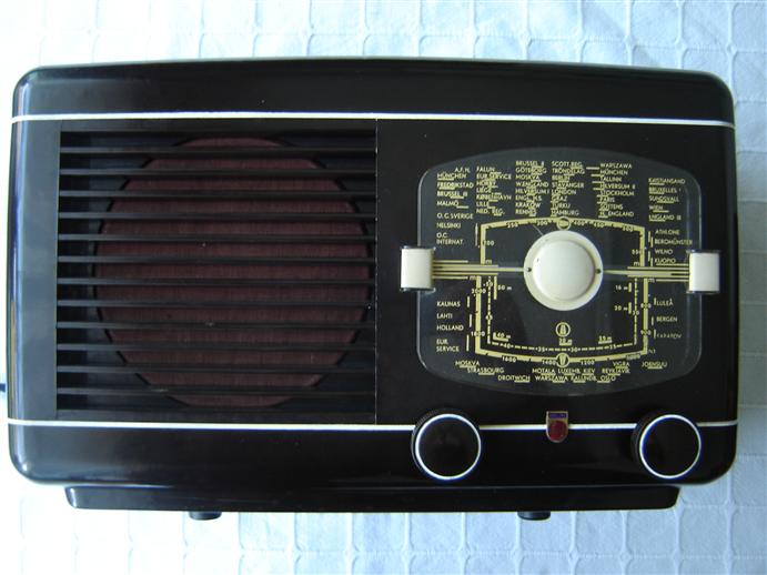
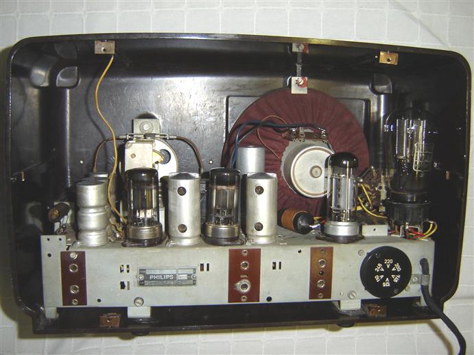
BX380A
Manufactured in 1948
Tubes: ECH21, ECH21, EBL21, AZ1
|
|
 |
 |
|
 |
 |
|
BX373A
Manufactured in 1948
Tubes: ECH21, ECH21, EBL21, AZ1
|
BX490A Manufactured in 1949
Tubes: ECH21, EAF42,EAF42,
EBL21, EM34, AZ1
|
 |
 |
|
 |
 |
|
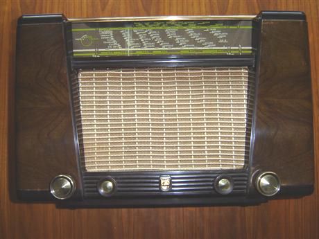
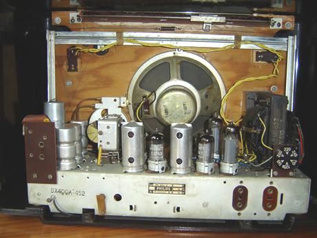
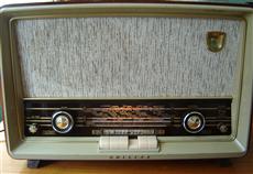
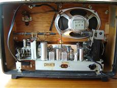
BX400A Manufactured in 1950
Tubes: ECH42, EAF42, EBC41, EL41, AZ41
|
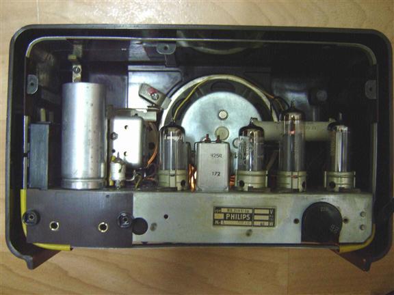
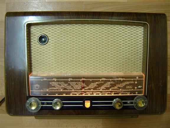
BX210U Manufactured in 1951
Tubes: UCH42, UF41, UBC41, UL41, UY41
|
 |
 |
|
 |
 |
|
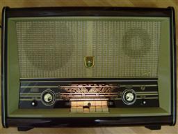
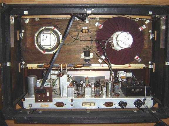
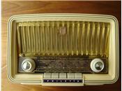
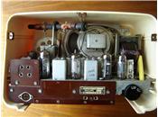
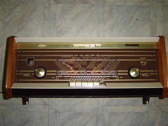
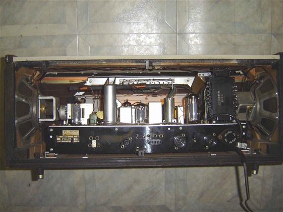
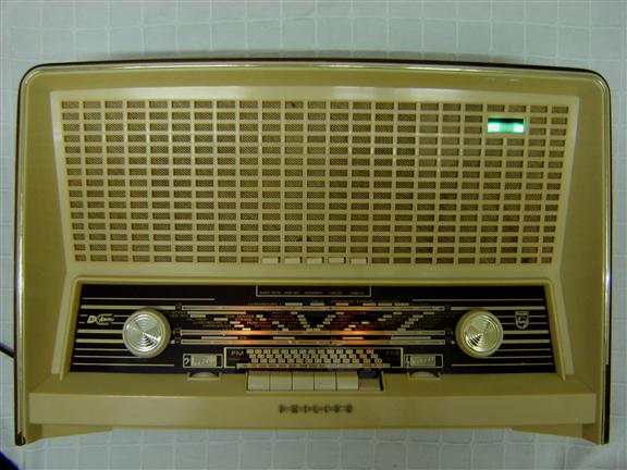
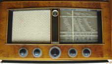
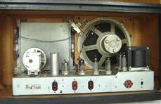
BX410A
Manufactured in 1951
Tubes:
ECH42, EAF42, EBC41, EL41, AZ41, EM34
|
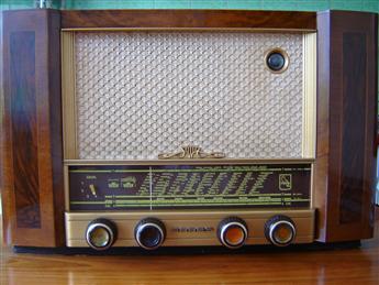
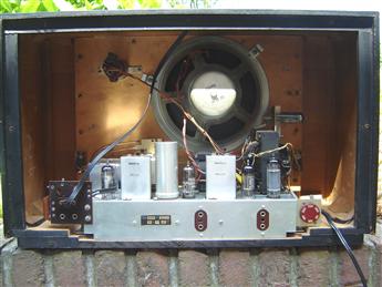
BX533A
Manufactured in 1954
Tubes:
EC92, EC92, EF85, ECH81, EF41, EABC80,
EL84, EZ80, EM34
|
 |
 |
|
 |
 |
|
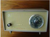
B5X63A Manufactured in 1956
Tubes: ECC85, ECH81, EF89, EF85, EABC80
EL84, EL86, EZ80, EM80
|
B5X72A Manufactured in 1957
Tubes:
ECC85,ECH81,EF89,EF85,EABC80,EL84,EL86,
EM80,EZ80
|
 |
 |
|
 |
 |
|
B2D03A Manufactured in
1960
Tubes: ECC85, ECH81, EF89, EABC80, EL95
|
B0X15U
Manufactured in 1961
Tubes: UCH81, UBF80, UCL82, UY89
|
 |
 |
|
 |
 |
|
B5X14A Manufactured in
1961
Tubes: ECC83, EAA91, ECC85, ECH81, EF89,
EBF89, EL84, EL84, EZ81, EM80
|
B5X82A
Manufactured in 1958
Tubes: ECC85, ECH81, EF89, EF85,
EABC80, EL84, EL86, EZ80, EM84
|
1.2 Philips power supply units and rectifiers
 |
|
 |
|
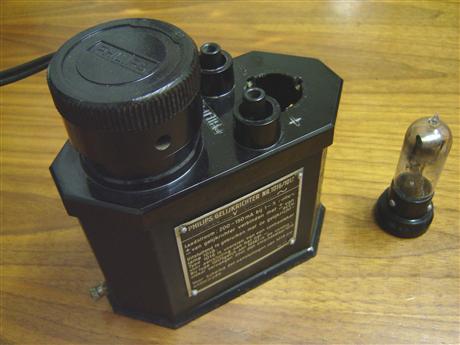
Rectifier model 1017
Manufactured in 1929
Tube: Mercury rectifier 1018
|
Power supply
model 372
Manufactured in 1925
Tube: Rectifier 373
|
 |
 |
|
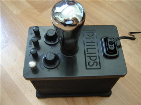
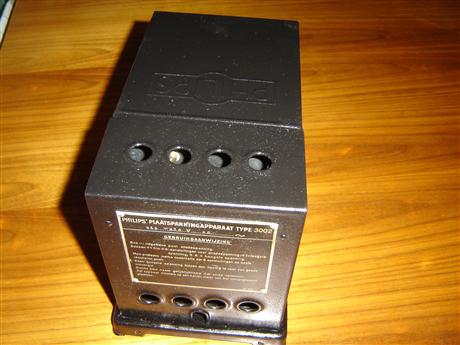
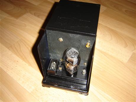
Power supply
model 3002
Manufactured in 1928
Tube: Rectifier 1805
|
 |
 |
|
Rectifier model 327
Manufactured in 1925
Tubes: Mercury rectifier 328 and
stabilization resistor tube 329
|
1.3 Erres Radios
 |
 |
|
 |
 |
|
KY509
Manufactured in 1950
Tubes:
ECH42, EF41, EBC41, ECC40, EL41, EL41,
EM34, AZ41, AZ41,
|
KY537
Manufactured in 1953
Tubes:
ECH81, EF85, EABC80, EC92, EL84, EM34, EZ80
|
1.4 Fridor Waldorp Radios
 |
 |
|
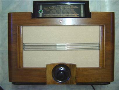
Waldorp 502 Manufactured in 1949
Tubes: ECH21, ECH21, EBL21, AZ1 |
1.5
Belgian Radios
 |
 |
|
350A from SBR
Manufactured in 1939
Tubes: ECH3, EF9, EBL1, AZ1
|
1.6
German Radios
 |
 |
|
 |
 |
|
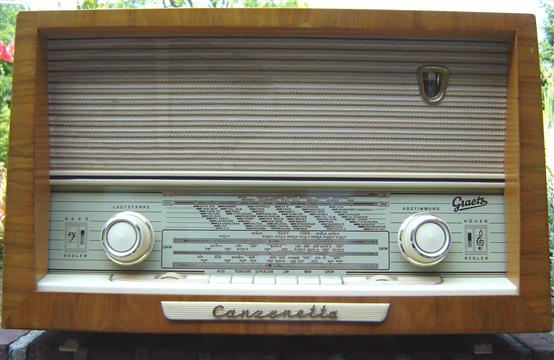
Graetz Canzonetta 515
Manufactured in 1957
Tubes: ECH81, EF89, EABC80, EM80, EL84
|
Nordmende Stradella
Manufactured in 1963
Transistors:
AF106, OC615, AF105, AF105, AF105,
AC162, AC162, AC152, AC152
|
1.7
Homemade Radios
 |
 |
|
 |
|
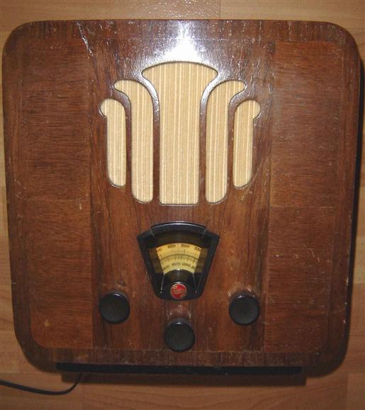
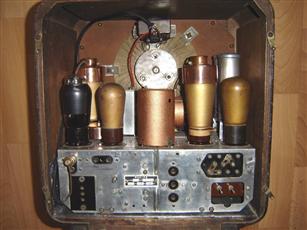
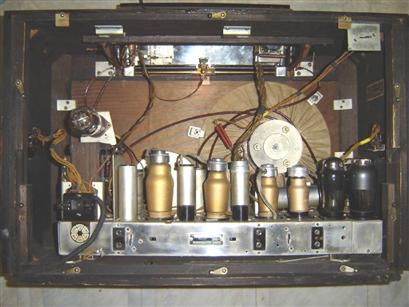
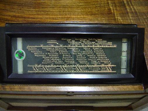
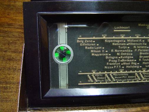
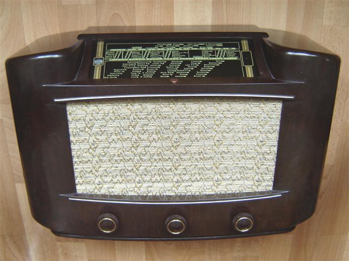
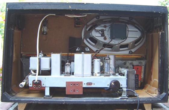
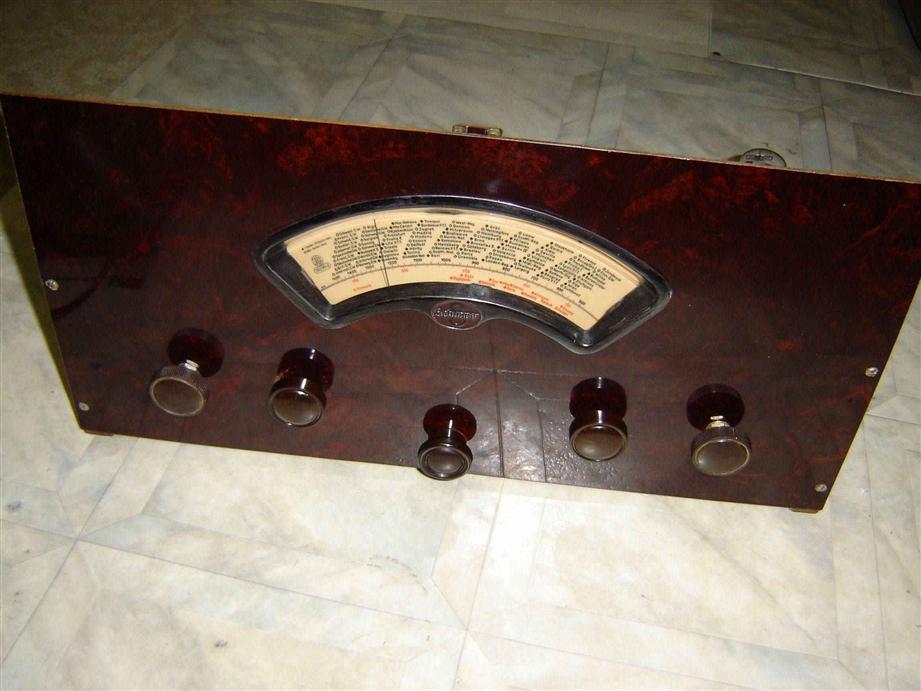
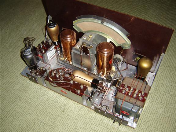
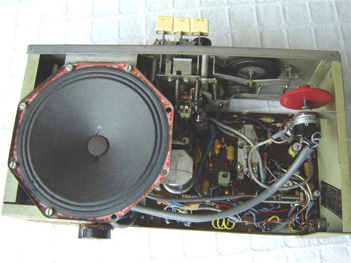
Schaaper
radio manufactured in 1931
RF tube:
E452T
Detector tube: E446
LF Amplifier tube: E443H
Rectifier tube: 1823
|
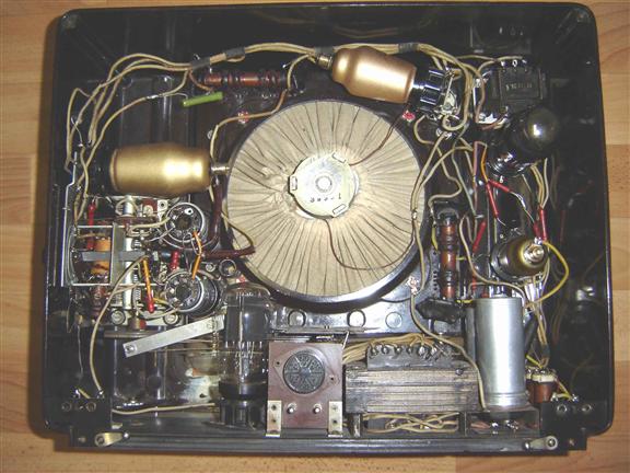
Schaaper single knob tuning-unit
|
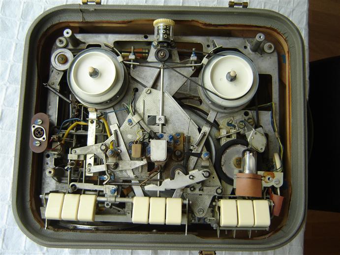
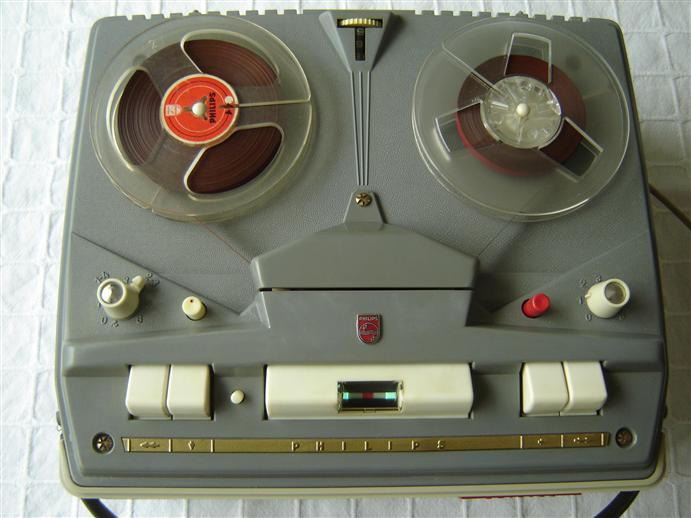
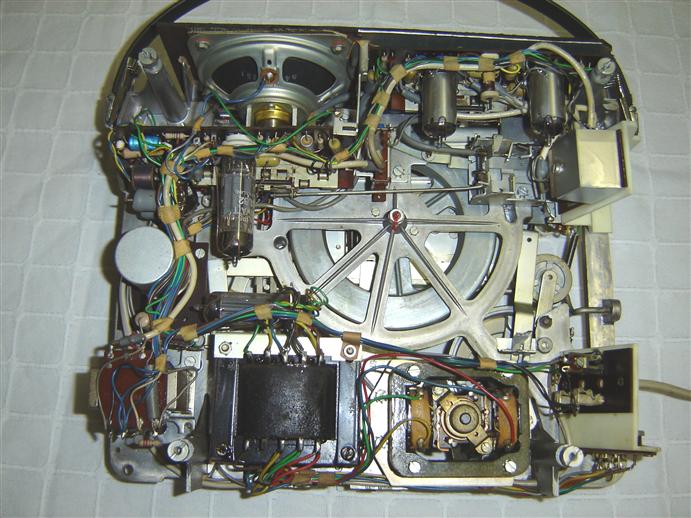
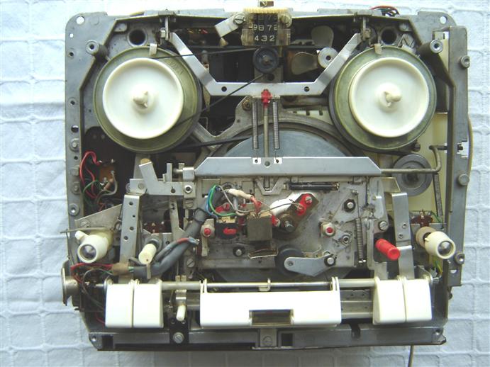
1.8 Philips Tape
Recorders
 |
 |
 |
|
EL 3516
Manufactured in 1958
Tubes: EF86, ECC83, ECL82, EM81, EZ80
|
 |
 |
 |
|
EL 3541
Manufactured in 1961
Tubes: EF86, ECC83, ECL82, EM84, EZ80
|
 |
 |
|
|
|
|
EL 3514
Manufactured in 1962
Tubes: ECC83, DM71, EL95
|
|
1.9 Philips Televisions
 |
 |
|
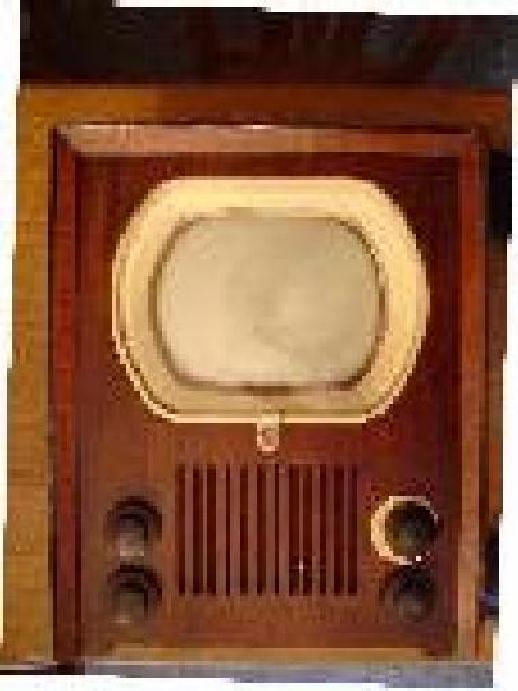
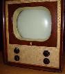
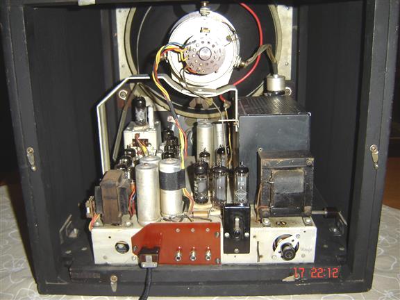
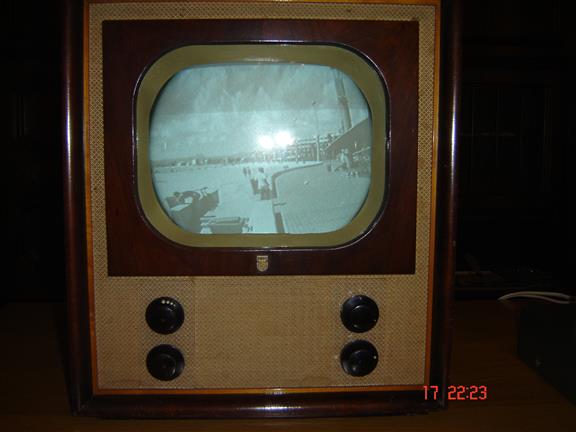
TX400U Manufactured in 1950
Tubes:
MW22-16, 2xPY82, 9xEF80, EQ80, EL42, 2xEB91, PL83, 3xECL80,
PL81, PY80, EY51
Note: The picture
on the right shows the TX400U in operation connected to the Philips TV Service Generator GM2891/50 !
|
 |
 |
 |
|
TX500U Manufactured in 1951
Tubes:
MW31-74, 2xPY80, 9xEF80, EQ80, EL42, EB91, PL83, 3xECL80,
PL83, PY80, EY51
Note: The picture
on the right shows the TX500U in operation !
|
Chapter 2 Renovation
hints for radios
2.1 General
These renovation hints are primarily
intended for the technical part of the radio. It is assumed that the
housing and the chassis have been thoroughly cleaned and are not damaged.
In case the housing has been severely scratched it can be
renovated by using the French polishing method. French polish is frequently used as the only finish on wooden
housings or cabinets because it can be completely controlled and
made to sit on top of the wood rather than to soak into the wood
which would change the resonance of the wood molecules. However,
keep in mind that this process is very time consuming and needs
quite some patience.
For those who do not have that patience, you can use a much faster
method by using high polish floor varnish that also yields an
excellent result.
To be successful, the housing must be grinded first using 180-grit
sandpaper, then 220 grit, then 400 grit and finally 600 or even 1200
grit. After this grinding process the French polish or floor
varnish can be applied.
As far as the chassis is concerned, the best way to clean this is by using
benzene. I would not recommend the use of
copper polish since it will affect the cadmium layer on the chassis
and will leave a dirty shiny appearance on the surface of the
chassis.
With respect to the station scale I can be very short: do never
touch the backside of the scale! Just wipe off the dust with
a dry cotton cloth. However, the front side can be cleaned by using
a mild detergent. Once again, never apply this to the backside of
the scale. Unfortunately, I have experienced 2 blank station scales by
employing this process.
Fortunate enough I have been able to procure the original station scales again at "Marktplaats"
on the Internet.
2.2 Components
2.2.1 Electron tubes
Electron tubes, or valves, can be tested with the aid of a tube tester.
Tests should be performed on mutual conductance, gas in the tube and
electrode shorts.
Usually, the emission has drastically decreased which results
in a decrease of mutual conductance by even a factor of 2.
However, in most cases this will not result in a strong reduction of
sound quality.
You often will see that the tube is completely dead with the
exception that the filament still glows.
In most cases this is caused by a loose connection in the tube
socket. To solve this problem, you can remove the socket from the
glass tube by making a circular saw cut in the socket at a distance of 5 mm from
the glass. Then longitudinal to the tube cut the small ring with a
saw. Put a screwdriver in this newly created slit and break the
socket off and remove the remainders of the socket. Be careful not
to break the wires that extend through the glass.
Take a tube that is not used anymore and remove the glass. Do not
damage the socket since you have to use it again on the tube to be
repaired. For safety reasons, first make a small incision in the
glass using a small diamond grinding tool to remove the vacuum in the
tube. Remove the glass, the brownish adhesive and wires from the
socket and make sure that the holes in the socket pins are open.
After having extended the wires, put the socket on the tube and
solder the wires into the socket pins. To alleviate the mounting of the socket, the wires are cut at
a different length which will ease the assembly of the wires in the
socket pin holes. To properly attach the socket to the glass, two components adhesive can be used.
When repairing shielded tubes, make sure that the wire connected in
parallel to the cathode or is connected to an extra pin, is properly
secured and connected to the shielding.
2.2.2 Resistors
Certain types of resistors, especially these, do
drift in time with respect to resistance value. Some of them might
even be ruptured thus forming an open circuit. Particularly, drifted
resistors that are used to provide the voltage bias for the electron
tube should be replaced to improve the performance of the radio.
2.2.3 Capacitors
Usually, the electrolytic capacitors that are used to smooth
the ripple on the rectified voltage have a high leakage current and
should be replaced. To do so, open the capacitor by carefully
bending back the swaged aluminum side of the capacitor and remove
the inner material. Put a new capacitor inside the aluminum tube and
close the capacitor.
Be sure that the polarity of the new capacitor is correctly
connected to the terminals.
The well known black tar Philips capacitors will always show a drift
in capacitance value and may have a high leakage current. As a matter of
fact, I have measured leakage current values in the order of milli-amps at a test
voltage of 200V.
With respect to capacitors used for smoothing anode and screen grid supply voltage,
a leakage current of 100-200 micro-amps at a test voltage of 200V is
acceptable.
For coupling capacitors, a leakage current greater than
10 micro-amps is not acceptable since it will heavily influence the
bias of the next electron tube which is manifested in an increase in
grid bias voltage.
In those cases where the black tar capacitors need to be replaced, operate as
follows:
Take a pertinax tube having the same dimensions of the old tar
capacitor and assemble a new capacitor having the correct
capacitance and working voltage inside the pertinax tube (see
picture).
On forehand, the connection wires of the capacitor have been replaced
by wires that have the same diameter of the old capacitor. Today's
capacitors are much smaller in size and hence have thinner
connection wires.
At the left and right side of the pertinax tube, 2 lathe machined
delrin rings are attached that have been tapered at an angle of 120
degrees (see picture). After painting
the whole assembly with black satin paint, the capacitor is ready for
use and cannot be distinguished from the old black tar capacitor (see
picture).
2.2.4 Variable tuning capacitors
Use a small soft brush to remove the dust from the tuning capacitor. Be careful not to bend the thin aluminum
plates.
Although the thin aluminum plates look somewhat distorted and bended, be careful not to bend
them.
I have experienced that at an old TV tuner. Apparently, all the plates
were bended so I thought this could not have been the intention
of the manufacturer. Hence, I decided to put the plates back in a
lined up and straight position again.
After that time consuming exercise I have never seen a picture
anymore on that TV set.
2.2.5 Coils
Measure the resistance of the coil and check whether the
resistance is in accordance with the specification in the service
documentation. Generally, coils do not need any specific attention because they
often are protected by an aluminum tube and the trimming core has
been secured against inadvertent adjustment.
So called honeycomb coils need to be made dust free only. Be
careful not to break the thin connection wires.
2.2.6 Rotary switches
Check that all contacts operate correctly by looking at their
elastic movement. If no movement is observed and ohmic resistance
measurements indicate no contact, carefully adjust or bend the
contact.
In case the rotary switch still makes intermittent contact, use
contact cleaning spray. Remove superfluous cleaning fluid.
2.2.7 Oscillator frequency
In the event of a bad reception on one of the wavebands in the
radio, for instance the medium wave, it is highly recommended to
check the frequency of the oscillator.
The medium waveband has got a frequency range of 513 kHz to 1714 kHz.
Assuming that the intermediate frequency of the subject radio is 473
kHz, then the frequency of the oscillator should vary between 986
kHz and 2187 kHz. In case the measured frequency of the oscillator
strongly deviates from these calculated values, the most probable
cause is a drift or even a defect in one of the capacitors in the
oscillator circuit that determines the oscillator frequency.
Chapter 3 The evolution of the radio tube
3.1 Introduction
We have to make a big step back in history
to the era of the wireless telegraphy in order to understand and map
the evolution of the radio tube.
In principle, the wireless telegraphy is based on scientific
experiments of Heinrich Hertz who demonstrated and proved in 1888 that electrical
oscillator waves generated in objects, could also induce electrical waves in objects that
were placed at a certain distance from the oscillating object.
Hertz demonstrated by means of his magnificent experiments that
these so called electromagnetic waves propagated with a speed that
was equal to the speed of light being 300000 km/sec.
Based on these very important experiments of Hertz, experiments which
served the purpose of proving Maxwell's assumptions, the wireless
telegraphy was born.
3.2 The electromagnetic spectrum
An electromagnetic wave in fact consists of two perpendicular waves
that propagate in a vacuum atmosphere at a speed of 300000
km/sec.
One component of the electromagnetic wave constitutes an electrical
field while the other component of the electromagnetic wave
constitutes a magnetic field.
One of the most well known forms of an electromagnetic wave is the
visible light. It distinguishes from all other electromagnetic
waves by its frequency. Amazingly, the visible light encompasses
only a very small part of the total electromagnetic spectrum.
(Click here to visualize the total electromagnetic
spectrum)
3.3 The very first radio tube
It has been the great merit of Marconi that he converted the invention
of Hertz in such a way that it was suitable for practical use. He
applied the necessary practical changes to the laboratory experiments
of Hertz that eventually resulted in an improvement in transmission
distance of up to 10 to 20 km at which distance he could exchange
Morse code signals by means of electromagnetic waves.
During these experiments, he replaced Hertz's electrical resonator by
a much more sensitive instrument called the coherer of professor
Branley and so he achieved substantial favorable results.
The coherer of Branley consisted of an evacuated glass tube that was
partly filled with metal particles loosely confined between two silver
plugs containing connection wires. If this instrument is placed in an
electric circuit employing a voltage source and a galvanometer, it
will show a high resistance to the electrical current in normal
condition.
However, if this device is subjected to electromagnetic waves, the
high resistance will suddenly decrease and the galvanometer needle
will noticeably deflect. Unfortunately, due to insufficient
sensitivity as detector, the coherer had a very short life.
In the following years, the detectors such as the Marconi detector and
the electrolytic detector, that were well known at that time, have
been replaced by crystal detectors. It was discovered that crystals
such as carborundum silicon and copper pyrite had the property of
conducting electromagnetic waves only in one direction. In this way,
the rectified high frequency currents could be made audible by means
of a suppression capacitor and a headphone.
Ultimately, the crystal detector appeared to be very unreliable
because of the fact that it required continuous adjustment and hardly
contributed to amplification of the signal.
The great break through came when Lee de Forest started his
experiments in 1906. These experiments resulted in the very first
radio tube called Audion (audio-ion).
During these experiments, Lee de Forest found that, when gas in a low
vacuum glass tube was heated by means of a filament inside the tube,
the gas became conductive in only one direction. By winding a wire
around the glass tube and applying a high frequency signal to this
wire, the current flow in the glass tube could be adjusted.
In his original design, a metal plate and a filament were melted into
the glass tube. The metal plate was connected to the positive terminal
of a 22 Volt battery via a headphone.
The negative terminal of the
battery was connected to one side of the filament. A high frequency signal connected to the wire that was wound around
the glass tube, caused a fluctuating current in the headphone.
A rather logical subsequent development of the Audion resulted in a
glass tube in which the wire that was formerly wound around the tube,
had now been positioned inside the glass tube.
Various scientists such as John Ambrose Fleming, Edwin Armstrong en
Irving Langmuir have been involved in the improvement activities of
the Audion.
The improvements were particularly aimed at removing the gas in the
tube and thus improved the vacuum condition in the tube.
This was in contradiction as to what the patent of Lee de Forest
described: "The gas in the tube is essential for the correct
functioning of the tube".
In fact, the Audion was yet meant to function as detector while
Langmuir's high vacuum tubes were supposed to function as amplifier and
remained proper functionality at much higher frequencies.
Ironically, the Audions that had lost their demodulating properties
due to the absorption of gas by the metal electrodes and thus were
identified as defective, virtually changed into an amplifier but
nobody did realize it at that very moment.
3.4 The first Dutch radio tube
If we have to believe the words of Leonard Bal's son, we learn
that his father was the inventor of the first radio tube in Holland. How
could we otherwise explain the strange events that
occurred during the first Dutch radio exhibition in 1918 at The Hague.
The visitors of the exhibition truly could receive Morse signals from
radio receivers, however, exclusively via headphone and without
amplifier.
However, all of a sudden, at exhibition stand number 33 occurs a tiny
miracle. There is Leonard Bal, director of the Bal Electro technical Company from Breda, standing in his stand next to his self-made
wireless receiver that contains the very first Dutch radio tube that
enables amplification of ether signals.
He is even capable of resounding the time signal from Paris through
the exhibition hall. The competitors are speechless.
Where the big high tech shots like Philips did fail, a relative
unknown outsider indeed succeeded in amplifying radio signals. Leonard
Bal had to be world-famous now, unfortunately, it didn't go that
way.
The son of Leonard Bal continues his story: "Strange
events had happened in 1918. My father was envied his success.
At the end of the first day of the exhibition, he went back to his
stand and stunningly discovered that his radio tube was
stolen.
The next day he went back to his stand and saw with great astonishment
that the radio tube was put back in the radio receiver. Subsequently, it is very strange that
two months later, Hanso Idzerda, who is a radio
technician and director of a radio factory, developed a radio tube that was identical to Bal's radio tube.
Moreover, Idzerda acquired the legal rights for a patent on this so-called IDEEZET
tube that was put into production by Philips as the first Dutch radio
tube.
However, rumors went on at that time saying that neither Idzerda nor Bal was the
first Dutchman who produced a proper functioning radio tube. It was
said that the truly
very first tube was made by glass blower
Hendrik Schmitz who was employed at the metal filament lamp factory
Holland in Utrecht. The following case did occur: On November 15 in
the year1917, a certain lieutenant Tolk and lieutenant commander at
sea Dubois visited the Holland factory. They had a Telefunken radio
tube with them that had been recovered from a German airplane that had
crashed near Kampen.
The Dutch Ministry of War ordered the factory to produce a copy of the
tube under strict secrecy. Four days later, on the 19th of
November, glassblower Schmitz and laboratory worker Prinsen had
finished a first functioning radio tube.
Early 1918, tube factory Holland had finished their own radio tube
that was a predecessor of the radio tubes that, until 1923, had been
used in radio receivers of the "Nederlandse Seintoestellen
Fabriek NSF" in Hilversum. NSF stood at that time for Dutch
Signaling apparatus Factory.
Then, also in the beginning of 1918, Idzerda got a hunch of the
experiments that took place in Utrecht. He tried to order some radio
tubes at the Holland factory. However, the Dutch military authorities
did put a stop to it.
Yet in March 1918 at the radio exhibition in The Hague, Idzerda
showed an old-fashioned crystal receiver. There was also lieutenant
Tolk who demonstrated a receiver that he had built using radio tubes
that came from the secret Holland series.
The interior of the apparatus was officially state-secret and
therefore it was hidden in a sealed cabinet.
Bals's receiver that stood somewhat further away, was not more than a
wired circuit on a bare wooden board.
This frankness and openness did draw enormous attention. The radio
tube that had ground glass to hide the interior of the tube was
labeled as "Bal-Pope Venlo" while nobody knew that this
factory in Venlo manufactured already radio tubes.
As was said earlier, strange things did occur at The Hague. Bals's
radio tube disappeared on the first evening of the exhibition and next
morning it was installed again in the radio as if nothing had
happened.
Bal did not give much rumor to the incident and kept it silent. On
the contrary, the brutal theft of Tolk's box containing spare parts was front-page news.
Soon after that, Bal was confronted with overwhelming competitors. In
Hilversum, the NSF started manufacturing wireless receivers containing
Holland radio tubes and the Philips Company Archives show that there
are papers present that give evidence that Idzerda received a radio
tube from Philips that was manufactured in accordance to his
specifications.
On 1 July 1918, an agreement was signed in which Idzerda was
obliged to buy a minimum of 180 "Ideezet" tubes per year.
Shortly thereafter production started.
Whether Idzerda had something to do with the mysterious events that
did occur in the first night of the radio exhibition in 1918 is
far beyond certainty.
For, in November 1917, Idzerda's later partner Philips had already been
approached by lieutenant Tolk with the Telefunken valve from Kampen.
Philips's technical staff was interested but Gerard Philips did not
see any business in radio-work that he called "militaire
spielerei". Not until Idzerda did guarantee purchase of goods, he
also approved.
Unfortunately, we will never know the details and the truth about all
this. What we know for sure is, that all this technological hassle has
ultimately led in the late twenties and early thirties, to good
quality wireless receivers in almost any household and stayed that way
until mid fifties of the last century when the transistor radio was
introduced.
In modern electronics, vacuum tubes have been replaced on a large
scale by the so-called "solid state devices" such as the
transistor that was invented in 1947 and has been implemented in
integrated circuits in 1959.
Nevertheless, vacuum tubes are still widely employed in
high-end audio applications. Tube amplifiers produce a wonderfully
warm tone that has not yet been successfully emulated through digital
technology.
3.5 The operation of the electron tube
3.5.1 Introduction
Radio broadcasting that started to prosper since 1920 urged for
mass-production of electron tubes.
The bright glowing tungsten cathode was very soon replaced by the soft
glowing oxide cathode and the screen grid tube made its entry.
Somewhat around the year 1935, the strive for size reduction of the
radio tube did start which very soon thereafter resulted in the fact
that the new tubes didn't have any resemblance anymore with the light
bulb.
Due to the fact that the "radio lamps" are now tube shaped
and their application has little to do anymore with radio, the name
electron tube is more appropriate.
3.5.2 The Diode
The modern electron tube is a high vacuum tube in which a current of
free electrons can be established. To facilitate movement of free
electrons, the inside of the tube should be evacuated.
The small amount of stray gas that might still be present in the tube is
removed by means of a so-called getter that is mounted inside the
tube. This getter is a small cup containing a bit of barium that
reacts with oxygen strongly and absorbs it. When the tube is pumped
out and sealed, the getter is heated by
means of high frequency energy thus producing a getter flash which
manifests itself as a silvery patch you see on the inside of the
glass. This
"mirror" absorbs the stray gas that is still present in
the tube and is also capable of some gas absorption when the tube is
normally used later on.
How does the electron current start inside the tube anyhow?
To answer that question, the tube should contain something that can
release electrons, the so-called cathode.
We know that conduction in metals takes place by means of free
electrons. These electrons can move freely throughout the metal because
they are not bound to certain atomic nucleus.
To release free electrons from the metal, energy is required in order
to overcome the one-sided attractive power of adjacent positively
charged atoms.
This so-called release energy is determined by the charge of an
electron multiplied by the potential difference the electron passes
through. This potential difference is called the release voltage.
Electrons can acquire the required
energy to overcome the release voltage by heating the metal thus
leading to thermionic emission.
 The cathode now, consists of thin tube covered with barium and
strontium oxide. A filament, which is covered with aluminum
oxide, is mounted inside this tiny tube. The purpose of the aluminum
oxide is to prevent shortage with the cathode.
The cathode now, consists of thin tube covered with barium and
strontium oxide. A filament, which is covered with aluminum
oxide, is mounted inside this tiny tube. The purpose of the aluminum
oxide is to prevent shortage with the cathode.
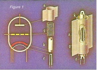
See figure 1 in which:
f
is the filament
k is the cathode
a is the anode
g is the grid (see paragraph 3.5.3)
If the filament is heated, thermionic emission will cause the cathode
to release electrons.
When a metal plate, the anode, is placed at some distance around the
cathode, we call it a diode. See figure 2.
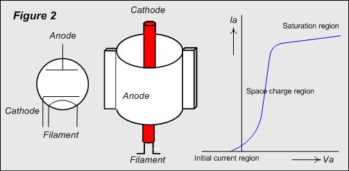 When there is no voltage applied between anode and cathode, yet a
small amount of electrons will leave the cathode. Some of them will
reach the anode and cause a negative charge on the anode. The other
electrons will surround the cathode as a cloud of electrons. This
causes a so-called space charge that prevents the cathode from
releasing more electrons.
When there is no voltage applied between anode and cathode, yet a
small amount of electrons will leave the cathode. Some of them will
reach the anode and cause a negative charge on the anode. The other
electrons will surround the cathode as a cloud of electrons. This
causes a so-called space charge that prevents the cathode from
releasing more electrons.
If we connect now a current measuring device between the anode and the
cathode, electrons will return from the anode to the cathode and the
needle of the measuring device will deflect.
If we apply a negative voltage between the anode and the cathode, this
current will be diminished and at a sufficient negative voltage, this
current will even completely disappear. Usually, this occurs at a
voltage of -0,1 to -1,5 Volt.
The region between 0 to -1,5 Volt is called the initial current
region. See the curve on the right in figure 2.
However, if we apply now a sufficiently positive voltage between the
anode and cathode, a great amount of electrons will flow from cathode
to anode thus causing a so-called negative space charge. This negative
space charge causes the potential in the vicinity of the cathode to
decrease or even gets negative. This space charge region hampers the
release of new electrons.
However, with the increase in anode voltage, a positive effect on the
space charge region is observed and breaks the space charge down. See
picture 2.
When the anode voltage is even further increased, a point will be
reached at which the anode current hardly increases.
This is the so-called saturation region of the tube as depicted in the
graph in figure 2.
The space charge has now completely disappeared and all electrons that
have been released by the cathode have reached the anode.
3.5.3 The Triode
In the vacuum tube diode, there was no way of controlling the
amount of current flow in the tube. It was either conducting, or not
conducting.
When in the diode as described above, a spiral shaped wire
construction is placed between the cathode and anode, we call this
tube a triode. This wire construction is called grid. See g in figure
1 and figure 3.
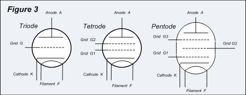 Thus the triode consists of three active elements, the cathode, the
grid and the anode. The current flow between cathode and anode can now
be adjusted by varying the voltage level on the grid. If a resistance
is placed between the anode and the high voltage supply, the voltage
variations at the anode is greater than the grid voltage variations,
thus, amplification takes place.
Thus the triode consists of three active elements, the cathode, the
grid and the anode. The current flow between cathode and anode can now
be adjusted by varying the voltage level on the grid. If a resistance
is placed between the anode and the high voltage supply, the voltage
variations at the anode is greater than the grid voltage variations,
thus, amplification takes place.
It is important to mention that control of the anode current occurs
without any delay.
As was implicitly mentioned before, anode current Ia depends on the
grid voltage Vg and supply voltage Vb.
The measured relationship between these parameters can be graphically
represented as depicted in figure 4 below.
The triode circuit that is underlying this graphical representation is
also shown in figure 4.
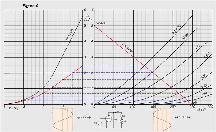
If we look at the circuit, we see that the power supply Vb is
connected to the anode through resistor Ra. The grid bias voltage is
-Vg, the anode-cathode voltage is Va and the anode current is Ia.
We now can write down the following equation:
Vb = Va + Ia×Ra or otherwise noted: Ia = -(1/Ra)×Va + Vb/Ra
The graphical representation of this equation is a straight line
determined by the coordinates Va=0,Ia=Vb/Ra and Va=Vb,Ia=0. (Compare
this with the equation for a straight line y=mx+q in which m is the
tangent of the angle formed by the straight line and the x-axis)
The point of intersection of the straight line with the various Vg
lines determines the value of the anode voltage Va and the anode
current Ia. This straight line is called the load line.
When we now vary the grid voltage Vg, the point of intersection will
move along the load line. The point of intersection is called the
operating point of the tube.
The amount of grid voltage variations and anode current variations can
graphically be determined as shown in the lower red curve of the left
graph in figure 4.
In figure 4, the grid has a fixed bias of -1 Volt. On this grid bias
voltage, a 1 Volt peak/peak sinusoidal signal has been superimposed.
By dragging the anode currents in the left graph to the intersection
points with the load line in the right graph, we will find the mating
anode voltage variations and naturally also the mating grid voltage
variations.
The lower red curve in the left graph of figure 4 that was used to
determine the variations in anode voltage by means of the load line
is called the dynamic Ia-Vg characteristic.
With the aid of this dynamic Ia-Vg characteristic we can easily
construct the static Ia-Vg characteristic.
To do so, we set the load resistance to zero which causes the load
line to be perpendicular to the Va axis.
By dragging the corresponding intersection points of the load line
with the Vg lines to the Ia axis and Vg axis in the left graph, we
derive at the static Ia-Vg characteristic. See upper black curve in
left graph of figure 4.
It is important to mention that these characteristics are valid for
only one supply voltage Vb.
From the characteristics in figure 4 we can deduct some very important
tube parameters.
Static mutual conductance: Sstat
= (ΔIa/ΔVg) at constant Va
Tube resistance:
Ri = (ΔVa/ΔIa) at constant Vg
Amplification factor:
μ = -(ΔVa/ΔVg) at constant Ia
These three parameters are interrelated by the equation: μ = Sstat×Ri
We can also calculate the relationship between the static and dynamic
mutual conductance.
Sdyn = dIa/dVg or dIa = Sdyn×dVg
For small signal changes we can write the equation Vb = Ia×Ra + Va
as follows:
dVa
= Vb - Ra×dIa hence dVa = Vb - Sdyn×Ra×dVg
The amplification factor μ is: dVa/dVg = -Sdyn×Ra
From the equations for the model of a triode, which are not further
discussed here, we can deduct that:
dIa = μ×dVg/(Ri + Ra) hence it follows that dIa/dVg = Sdyn
= μ/(Ri + Ra)
Due to the fact that μ = Sstat×Ri we can
calculate that Sdyn = Sstat×Ri/(Ri
+ Ra)
3.5.4 The Tetrode
Adding another grid to the triode, between the control grid and the
anode, makes it a so-called tetrode.
This grid, the screen grid indicated as G2 in figure 3, act as an
electrostatic screen between control grid and anode thereby reducing
the stray capacitance between control grid and anode by a factor of
1000 as compared to the triode.
Due to this reduction in stray capacitance, the retroaction from anode
to control grid is much smaller as is the case in a triode.
A second consequence of adding a screen grid is that the anode voltage
has hardly any effect on the total emission current i.e. the sum of
anode current and screen grid current.
The ratio of anode current and screen grid current is heavily
influenced by secondary emission of anode and screen grid causing the
Ia-Va characteristic of vintage tetrode tubes to have unpleasant
irregularities as can be seen in figure 5 below.
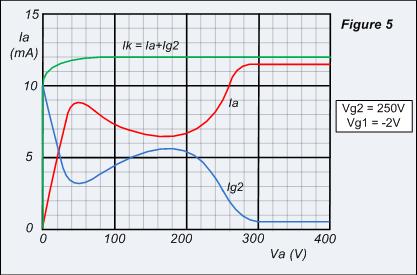
The curvature in this graph limits the use of the tetrode for those
anode voltages that are greater than the screen grid voltage.
If no anode voltage is applied, the total cathode current will flow to
the screen grid and the anode current is zero. For small positive
anode voltages, the anode current will rapidly rise with increasing
anode voltage. The bulk of the electrons will flow through the meshes
of the screen grid to the anode.
However, due to the low anode voltage, the energy of these electrons
is too low to cause secondary emission. If we now increase the anode
voltage, electrons that hit the anode will cause secondary emission.
These electrons are located in the region between the anode and screen
grid and will move towards the electrode that has the highest
potential i.e. the screen grid. Hence, the screen grid current will
increase and the anode current will decrease. The secondary emission
can even get that large that the lowest part of the curve will cross
the horizontal axis.
If we make the anode voltage larger than the screen grid voltage, the
secondary electrons will return to the anode. Part of the primary
electrons though, may reach the screen grid and will free secondary
electrons. These electrons will move to the anode thus increasing the
anode current.
With respect to anode voltages greater than the screen grid voltage,
the anode current is fairly constant.
From the Ia-Va characteristic it can be concluded that for anode
voltages greater than the screen grid voltage, the tube resistance is
very high. The mutual conductance is, assuming equal dimensions,
somewhat smaller than the mutual conductance of the triode because
there will always flow some current to the screen grid.
The amplification factor μ, that is equal to Sstat.Ri, is
also much larger than that of a triode.
3.5.5 The Penthode
If we add a third grid to the tetrode, we call it a penthode. This third
grid is called a suppressor grid and is inserted between the anode and
the screen grid. The suppressor grid is a wide mesh like grid held at
a low potential since its only job is to collect the stray secondary
emission electrons that bounce off the anode.
The suppressor grid, identified as G3 in figure 3, is usually
internally connected to the cathode
It appears now that, at normal bias conditions of the tube, the anode
voltage has minor effect on the anode current, in other words, the
tube resistance is very high.
The penthode characteristics are shown in figure 6 below.
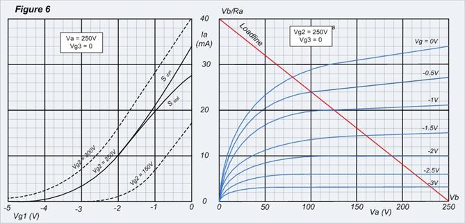
It is important to mention that the Ia-Va graphs on the right side of
figure 6 are valid for one particular screen grid voltage, in this
case 250 Volt. The graphs on the left side of figure 6 show that the
screen grid voltage heavily determines the anode current. The dashed
lines show this dependency very clearly for screen grid voltages of
150 Volt and 300 Volt.
Notice also that at a screen grid voltage of 250 Volt the static and
dynamic Ia-Vg characteristics hardly differ from each other.
Both the static and dynamic characteristics have been derived from the
Ia-Va characteristics. As a matter of fact, the Ia-Vg curves for 150
Volt and 300 Volt respectively have not been derived from the Ia-Va
curves because the curves in the right graph of figure 6 are only
valid for a screen grid voltage of 250 Volt.
3.6 The invention and the evolution of the transistor
Introduction
The history of the invention of the transistor is an interesting
story. In 1945 Mervin J. Kelly, "Director of Research" of Bell
Laboratories, had the objective to drastically improve the unreliable
telephone system of AT&T by employing electronic switching and
better amplifiers.
Vacuum tubes were not very reliable at that time because
they generated a great deal of heat and, particularly, because filaments
burned out and the tubes had to be replaced.
In 1945 a solid-state physics group was formed that had the major
objective to develop a solid-state amplifier.
The meaning of solid-state here was all that had to do with
semiconductor technology.
In 1947, John Bardeen en Walter Brattain, who formed a part of that
working group, discovered during their general research on
semiconductor materials that, when two closely spaced metal point were
pressed into the surface of a piece of semiconductor material, this
configuration had amplifier properties.
Shockley, who was in charge of this research work, demonstrated
shortly thereafter that, based on theoretical considerations, these
amplifier properties could also be evoked by attaching a piece of
p-germanium to both sides of a thin disk of n-germanium. What p and
n-germanium is will be discussed in chapter 3.6.2. This new
amplifier element was called transistor (composition of transformer
and resistor).
The first type was called point-contact transistor named after the two
metal points that were used and the second type was called junction
transistor.
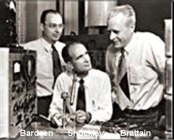 The
point-contact transistor has only led a very short life, however,
shortly thereafter, the junction transistor has been produced in very
large numbers. The
point-contact transistor has only led a very short life, however,
shortly thereafter, the junction transistor has been produced in very
large numbers.
The very fast distribution of the transistor is not that strange if we
consider that the transistor, like the radio tube, possesses amplifier
properties, though it is much smaller in size on the other hand.
Having the advantage of a smaller size, not yet all advantages of the
transistor have been mentioned.
As we saw in the electron tube, the amplification property was based
on control of electrons that, however, first needed to be released
from the cathode. In the transistor however, these electrons are
already available by nature, hence, no additional external energy is
required to free the electrons.
A filament in the transistor is totally superfluous causing that the
efficiency of the transistor to be much higher than the efficiency of
an electron tube. Furthermore, an electron tube requires for its
operation a supply voltage that is higher than ten volts whereas the
transistor operates at a voltage as low as 1 Volt.
Because of this low supply voltage, the power dissipation in a
transistor is substantially lower than it is in an electron tube.
Yet, apart from these advantages, the transistor has some disadvantages
such as the temperature dependency of certain transistor parameters.
Although it is possible to take measures against this drawback, the
maximum temperature at which germanium transistors can be operated is
limited to 8o°C. In the case of a silicon transistor, this
maximum operating temperature is somewhat around 150°C.
Another disadvantage in this initial period of the transistor was the
difficulty to produce transistors that had acceptable and useful gain
properties at very high frequencies. This characteristic of the
transistor has drastically been improved in the last decennia in the
20th century due to the strongly improved manufacturing
processes.
Also a big disadvantage of the transistor is its susceptibility to
high temperatures and high voltages. When a transistor is used at high
junction temperatures it is possible for regenerative heating to occur
which will result in thermal run-away and possible destruction of the
transistor. Due to improper cooling or bad design of the circuit in
which the transistor is used, the temperature may rise that high that
the gain factor and leakage current will increase which in turn will
increase
collector current even further.
Consequently, internal dissipation will further increase and this
regenerative process will eventually kill the transistor.
On the other hand, high voltages may lead to break-down between
junctions in the transistor causing immediate destruction of the
transistor. High voltages will also increase leakage currents that in
turn will increase the junction temperature that eventually will also
kill the transistor.
3.6.1 Semiconducting in germanium and silicon
During the discussion on thermionic emission in the electron tube it
was mentioned that conduction in metals is caused by free electrons.
These electrons can freely move around in the material, this in
contrast with the valance electrons in semiconductor material that are bound to specific ions.
In conductors, the concentration of free electrons is hardly dependent
on temperature. At absolute zero, the amount of free electrons does
not differ that much as that at room temperature.
On the other hand, semiconductors behave as perfect isolators at
absolute zero because all electrons are confined at their specific
places in the crystal lattice.
Germanium and silicon are typical examples of such a semiconductor.
From chemistry we know that a germanium atom is made-up of a
positively charged nucleus of 32 protons and 32 electrons traveling
within their respective orbits. The silicon atom's nucleus possesses a
positive charge of 14 protons and 14 electrons traveling also within
their respective orbits. The electrons traveling in their orbit,
possess energy since they are a definite mass in motion. Each electron
in its relationship with its parent nucleus thus exhibits an energy
value and functions at a definite and distinct energy level. This
energy level is dictated by the electron's momentum and its physical
proximity to the nucleus.
The closer the electron to the nucleus, the greater the holding
influence of the nucleus on the electron and the greater the energy
required for the electron to break loose and become free. Likewise,
the further away the electron from the nucleus the less its influence
on the electron. Outer orbit electrons can therefore be said to be
stronger than inner orbit electrons because of their ability to break
loose from the parent atom. For this reason they are called valence
electrons.
The outer orbit in which valence electrons exist is called the valence band.
These are the electrons from this band that are dealt with in the
discussion of transistor physics.
It is important to mention that both in the germanium and silicon
outer band a number of 4 valence electrons are in orbit.
These 4 electrons do have such a low energy level that they can easily
be freed from the valence band and become conduction electrons.
Germanium atoms and silicon atoms are what we call tetravalent and can
form crystals having a tetrahedron lattice structure in which each
atom is bound to 4 other atoms by covalent binding. In each bondage 2
valence electrons take part.
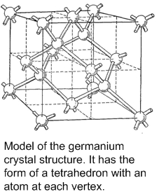 The figure on the right shows the positioning of the germanium atoms
in the tetrahedron lattice structure.
The figure on the right shows the positioning of the germanium atoms
in the tetrahedron lattice structure.
The spherical objects represent the germanium atoms while the bars,
connecting the spheres, represent the covalent binding.
If the temperature of semiconductor material is raised above absolute
zero, valence electrons may break away from the covalent bond due to
the acquired energy and will move through the crystal.
In principle, each isolator could become a conductor by applying this
theory, however, only the typical semiconductor materials like
germanium and silicon acquire a useful amount of conductivity already
at room temperature.
It is said that when the electrons break out off the covalent bond,
they enter the conduction band actually meaning the interval of
energies the electrons may have.
In order to break an electron loose from the covalent bond into the conduction band,
it requires at least an energy of qE. The chance that an electron
acquires this energy by thermal kinetic energy at a temperature T is,
like we saw at thermionic emission, also proportional with the Boltzmann-factor e-qE/kT.
In the case of pure germanium qE= 0,76 eV and in the case of
silicon qE= 1,12 eV.
At a room temperature of 300 oF, the factor kT has a value of somewhat around 0,025.
(k = 1.38 x 10⁻²³ Joule/oK = 8.616 x 10⁻⁵ eV/oK)
Note 1:
In physics the unit of energy, the Joule, is not very practical to
work with. Therefore, the electronvolt is used as unit of energy.
An electronvolt is defined as the amount of energy that an electron acquires when that electron, having a charge of 1,602.10-19
Coulomb, traverses a potential difference of 1 Volt.
From this definition we can conclude that 1 electronvolt = 1eV = 1,602.10-19 Joule.
Note 2:
In the next paragraphs, only
germanium will be discussed because the lecture material that is being
discussed is also applicable to silicon. In case differences, as far
as silicon is concerned, are applicable, they will specifically be
mentioned and discussed.
Due to the fact that qE has a much greater value than kT,
the Boltzmann-factor e-qE/kT will have a very small value
and is also very sensitive to small variations in E or T.
It appears that, already at room temperature, a useful concentration of electrons
in the conduction band is obtained when the value of qE is not much greater than
1 eV.
Each time a covalent bond is broken and an electron enters the conduction band, an
electron deficiency,
called a hole, is created at that particular spot where the electron
left the covalent bond.
In perfect pure germanium, the concentration nh
of these holes (number of holes per cm3) should be
equal to the concentration ne of the free electrons.
Even when very small impurities are present in the material, it may
occur that ne is equal to nh.
As long as this equality is true, the germanium is called an intrinsic
semiconductor (i-germanium).
Also holes can easily move through the germanium: namely, open spaces
can be occupied by valence electrons of the adjacent germanium atoms.
This movement of a hole can best be visualized by imagining having a
game in which 15 numbered tiles have to be moved across an area
consisting of 16 fields until they are lined up in the proper
sequence.
The tiles can be seen as the valence electrons while the single open
field constitutes the hole.
In every respect, the holes can be considered as positive
charged particles: for instance, under the influence of an electric
field, they will move through the material in a direction opposite to
that of the electrons.
As soon as the distance between a hole and an electron is in the order
of twice the distance between atoms, the binding force between the
hole and the electron is practically reduced to zero: the intermediate
material acts as an effective barrier. Therefore, one can assume that
electrons and holes, independently from each other, move freely
throughout the semiconductor material.
3.6.2 n and p Germanium
Conductivity in germanium semiconductor material can strongly be
increased by adding very small impurities of certain material.
When atoms of such impurities which have a different valence than
germanium, occupy the places of the germanium atoms in the tetrahedric grid, there will locally be a short or an
excess of valence electrons. Should the replacement impurity atom
contain 5 electrons in its valence band, which is specifically the
case for arsenic and antimony, 4 electrons will be used
to form covalent bonds with the neighboring semiconductor atoms. The
fifth electron is excess or extra.
This free electron has a weak bondage to the atom and is therefore
free to leave the parent atom and can easily enter the conduction band
(excitation energy is less than 0,1 eV).
We may state that, at room temperature, practically all excess valence
electrons have entered the conduction band.
Arsenic and antimony atoms in a germanium grid function as donors
of electrons. These electrons do not leave behind holes since the four
remaining electrons join covalently with electrons of the neighbor
atoms and thus satisfy the localized valency requirements. The donor
atom is therefore locked in position in the crystal and cannot move.
With the loss of the electron the donor's charge balance is upset
causing it to ionize. The donor impurity atom, therefore, can be
viewed as a fixed-in-position positive ion.
The conduction in germanium containing 5 impurity electrons in its
valence band is mainly caused by free electrons since the electrons
greatly outnumber the holes in the crystal.
The germanium crystal is negative in nature and is therefore called n-type
germanium.
Should, on the other hand, the replacement impurity atom contain only
3 electrons in its valence band, such as indium or gallium, all
three will be used up in covalent bonds with neighboring semiconductor
atoms. Since a lack of one electron prevails an empty space will exist
causing one bond to be unsatisfied. This empty space in the impurity
atom's valence band is called a hole and is positive in nature.
This empty space now can easily accept an electron from the germanium
crystal in order to satisfy the incomplete bond. This action results
in a moving hole and as in the case of the donor atom, this action
contributes to locking the acceptor in its lattice position, hence, it
cannot move.
The gaining of an electron upsets the acceptor's charge balance
causing it to ionize. Thus, the acceptor impurity atom, like the
donor, can also be viewed as a fixed-in-position ion, but one of
negative charge.
Since, in this case, a hole has been generated elsewhere in the
crystal, positive holes predominate and the material is called p-type
germanium.
Having understood the above, we can ascertain the following
important result: The doping of intrinsic semiconductor material not
only increases conductivity but also produces a conductor in which the
carriers in the conduction process are predominant holes or electrons.
In p-type material, holes predominating, are the majority carriers;
electrons the minority carriers. In n-type material, electrons
predominating, are the majority carriers; holes are the minority
carriers.
Concentrations of donor or acceptor atoms in the order of 1 per 109
germanium atoms constitute already a distinct change in conductivity.
To produce p- or n-germanium having well defined donor or acceptor
concentrations, it is required to start-off by producing pure
germanium followed by adding precise controlled amounts of donor or
acceptor impurities.
3.6.3 The p-n junction
There are various ways to create a precise defined borderline
between n-material and p-material in a germanium crystal. For
instance, if we solder at an accurate defined temperature an indium
contact to a piece of n-germanium and let the solder joint cool down,
a thin layer of the germanium will crystallize into p-germanium
underneath the solder joint. This is because some of the indium
material forms an alloy with the germanium. Note that the indium,
that is trivalent, functions as an acceptor.
The p-n junctions in most germanium layer diodes and germanium layer
transistors are made according this so called alloy process (alloy
junction).
Another way to create a p-n junction in a germanium crystal is the
so called crystal grow process. A single germanium crystal is grown by pulling it very slowly out of a melt of molten
germanium in which an excess of donor atoms (impurities) has been
added.
Now, a crystal of n-germanium is formed and while the grow process
continues, one can create a sudden transition to p-germanium by
adding an excess of acceptor atoms to the melt.
In that way a grown p-n junction is obtained.
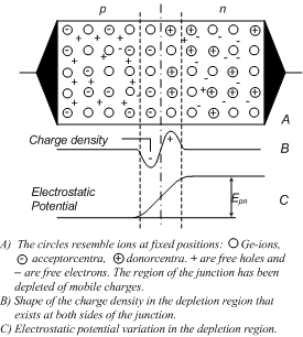 Across the p-n junction there exists a so called contact potential
that we can explain as follows (see picture on the right): As soon
as a p-n junction has been formed, holes from the p-germanium will diffuse to the right
across the junction to the n-germanium where they can recombine with the free electrons or they can diffuse back to the p-germanium. Due to the fact that right
from junction in the n-germanium free electrons disappear, there is left at that place an excess of
positively charged germanium ions; where on the left side of the junction holes
disappear, an excess of negative charge is formed. The areas of opposite charge
that as such do exist at both sides of the junction form a dipole layer in which the
concentration of mobile holes and electrons is much lower than outside that layer.
Across the p-n junction there exists a so called contact potential
that we can explain as follows (see picture on the right): As soon
as a p-n junction has been formed, holes from the p-germanium will diffuse to the right
across the junction to the n-germanium where they can recombine with the free electrons or they can diffuse back to the p-germanium. Due to the fact that right
from junction in the n-germanium free electrons disappear, there is left at that place an excess of
positively charged germanium ions; where on the left side of the junction holes
disappear, an excess of negative charge is formed. The areas of opposite charge
that as such do exist at both sides of the junction form a dipole layer in which the
concentration of mobile holes and electrons is much lower than outside that layer.
This
charge density is depicted in the figure on the right.
In practice the junction has a thickness of only half a micron.
Since the region of the junction is depleted of mobile charges, it is
called the depletion region.
At the junction, this depletion region evokes a strong electric field
that restrains the process of diffusion. This field adjusts
itself automatically such that, on an average per second, an equal
amount of holes will flow to the left as well as to the right.
At this equilibrium condition, a contact potential Epn (see
picture above) does exist across the p-germanium and n-germanium.
Holes that want to traverse the p-n junction from the left side to the
right side, must pass the potential barrier Epn; the
fraction of holes that have sufficient thermionic energy to achieve
this is always proportional to the Boltzmann factor.
There is also a hole current from right to left: all holes in the
n-germanium that diffuse towards the junction, fall-off the potential
barrier
Epn .
These holes constitute a current of which the amount of current does
not in the first place depend on the height of the barrier but solely
from the concentration of holes in the n-germanium.
This current is a saturated current. As long as the p-n junction
(diode) is not connected to any outside voltage source, both hole
currents must equalize resulting in a net hole current of zero.
However, when a voltage V is applied to the p-n junction such that the
p-germanium is made positive with respect to the n-germanium, then the
net hole current is no longer zero.
If we neglect the voltage drop across the germanium, the potential
barrier at the junction is reduced with the value V.
The equilibrium that was present at the p-n junction at the time no
voltage was applied yet, is now disturbed; holes will now flow from the
p-germanium to the n-germanium. This hole current will strongly
increase with V, however, the hole current from the n-germanium to the
p-germanium does hardly change since this is a saturated current as
already mentioned earlier.
Thus, this saturation current is not dependent on the voltage V but is
strongly dependent on the temperature.
The essential part in the characteristic behavior of a p-n junction is
that it constitutes a rectifier or in other words a diode. This diode
does conduct the current in only one direction and blocks the current
in the other direction.
 Nothing
has been mentioned so far with respect to the conduction of electrons,
this in order not to make things too complex. However, a similar
reasoning can be set up for the conduction of electrons. By adding the
hole current and the electron current we derive at a total current
that in the forward direction (V>0) strongly increases with V and
in the reverse direction (V<0) for small values of V
approaches the saturation current. Nothing
has been mentioned so far with respect to the conduction of electrons,
this in order not to make things too complex. However, a similar
reasoning can be set up for the conduction of electrons. By adding the
hole current and the electron current we derive at a total current
that in the forward direction (V>0) strongly increases with V and
in the reverse direction (V<0) for small values of V
approaches the saturation current.
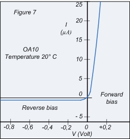
Figure 7 on the right illustrates the current-voltage characteristic
of a small layer diode.
By adding up the hole current and the electron current, we eventually
can set up an equation for the total current:
I = I0(eqV/kT - 1)
For T=300°K the value q/kT is in the order of 40.
If we assume that I0 = 0.3 μA, the curve fits
extremely well the given formula for the total current.
An important parameter we have to watch very carefully is the maximum
allowable voltage at reverse bias. If this value is exceeded, the p-n
junction will break-down and the diode is completely destroyed.
Before break-down occurs, the reverse bias current strongly increases.
An explanation for this phenomenon is that the thermionically created
charge carriers, which take care for conduction in reverse direction,
are that heavily accelerated by the reverse bias voltage that, when
they have crossed the p-n junction, they will break loose secondary
holes and electrons causing an acceleration of charge carriers. At
break-down, the acceleration factor will be "infinite".
It should be mentioned that the diode characteristic for a silicon
diode slightly differs from the characteristic of a germanium diode.
The forward voltage of a germanium diode at a specified forward diode
current lies between 0.2 and 0.5 Volt while in case of a silicon diode
the forward voltage lies between 0.6 and 0.8 Volt.
As far as the reverse voltage is concerned, it is much higher for a
silicon diode than for a germanium diode, however, the maximum voltage
is strongly dependent on the structure of the diode. Nowadays, silicon
diodes are manufactured that can withstand a reverse voltage of 1000-2000 Volts
while in the early days of the germanium diodes, this reverse voltage
was merely 50 Volts.
Furthermore, various parameters of the silicon diode are much less
temperature dependent than the parameters of a germanium diode.
3.6.4 The transistor
A junction transistor consists of a germanium (or silicon) crystal in
which a layer of n-germanium is sandwiched between two layers of
p-germanium. Alternatively, a transistor may consist of a p-type
germanium layer sandwiched between two layers of n-type germanium.
In the former case the transistor is referred to as p-n-p transistor
(see figure 8a), and in the latter case, as an n-p-n transistor (see
figure 8b).
Apart from showing the layer build-up, figure 8a and 8b also show the
representation of both types of transistors when employed in
electronic circuits.
The three portions of a transistor are known as emitter, base
and collector. The arrow on the emitter lead specifies the
direction of current flow when the emitter-base junction is biased in
the forward direction.
 Based
on what has been said in the previous sub-paragraphs about
semi-conducting and the behavior of p-n junctions, the principle of operation of a
transistor can easily be explained. Based
on what has been said in the previous sub-paragraphs about
semi-conducting and the behavior of p-n junctions, the principle of operation of a
transistor can easily be explained.
Figure 8c on the right shows a p-n-p transistor in which appropriate
voltages have been applied to the emitter and collector. When the
emitter is made somewhat more positive than the basis, a hole current
will flow from left to right through the p-n junction. We have
discussed that already in the layer diode.
For those holes that do not return again to the emitter, they will
diffuse over a certain distance into the base before they are
neutralized by conduction electrons.
In case the thickness of the base layer is much smaller as compared to
the average distance these holes can diffuse into the base, the
majority of the holes will reach the right n-p junction.
If the collector is biased negative with respect to the base, these
holes will be immediately "swallowed" by the collector.
In this way a hole current originating from one type of semiconductor
is transported right through a thin layer of an other type of
semiconductor.
This is in principle the operation of the transistor. Because there
are actually two types of mobile charge carriers (holes and electrons)
that take care of the conduction, this type of transistor is called a bi-polar
transistor.
The property that the emitter-base junction delivers current at a very
small positive emitter-base voltage and that current is collected at
the collector at a much higher negative voltage, does implicate the
possibility of amplification.
Because the hole current is a saturated current that reaches the
collector at a not too small negative collector voltage, this current
will thus not much be influenced by the collector voltage.
We call that a high output impedance. Similar to the penthode where we
saw that the anode current is not much influenced by the anode
voltage, we can obtain a large voltage amplification by inserting a
suitable resistor in the collector circuit.
Considering the emitter current Ie , part of that current
being αIe will reach the collector; the rest, (1-α)Ie,
flows into the base.
It should be explained here that the current amplification factor α,
that has usually a value in the order of 0.95-0.99, is the fraction of
the emitter current that reaches the collector.
At not too large values of Ie , α has a constant
value. In terms of the 4-pole substitution model for a transistor, α is called
the hfb parameter of the transistor.
As we can see in figure 8c, the base is common in both the input
circuit and the output circuit.
Therefore, this circuit configuration is called common base circuit.
However, the circuit that is mostly used is the common emitter
circuit. This circuit has got more favorable properties than the
common base circuit.
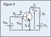 If
we look at figure 9 at the right we see a common emitter circuit using
an n-p-n transistor. We will demonstrate that in this configuration
current amplification takes place. If
we look at figure 9 at the right we see a common emitter circuit using
an n-p-n transistor. We will demonstrate that in this configuration
current amplification takes place.
Assume that Rb and Rc is set to zero. Referring to the common base
circuit we can state that IC
= hfb.IE and IE
= IB + IC
From both equations we can calculate that IC = hfb(IB
+ IC) = hfb.IB + hfb.IC
Hence: IC(1 - hfb) = hfb.IB
and IC/IB = hfb/(1 - hfb). In
the 4-pole substitution model for the transistor the term hfb/(1
- hfb) is called the dc forward current transfer ratio or
dc current gain of the transistor in common emitter configuration.
Suppose that hfb is equal to 0.98 then the current gain hfe
will be 0,98/(1-0,98) = 49 which is a considerable current gain.
To visualize the above, figure 10 shows the Ic-Vce characteristic of
an often used n-p-n transistor type 2N2222A and use the common emitter
circuit as shown in figure 9.
We set Vcc at 10 Volt and the load resistance Rc at 330 Ω.
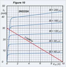 Note
that analogous to the electron tube we also can draw a load line in
order to determine the operating point of the transistor. Note
that analogous to the electron tube we also can draw a load line in
order to determine the operating point of the transistor.
Further notice that at higher collector voltages the curves tend to
show a slight upward inclination. The reason for this behavior is that
at higher collector-emitter voltages hfb
(or α) is not constant anymore but increases and hence also hfe
increases.
Let's assume that hfb increases from 0.995 to 0.996 (0,1%)
when Vce increases from a few Volts to 10 Volts.
The current gain factor hfe will change then from 0.995/(1-0.995) = 200
to 0.996/(1-0.996) = 250 which is an increase of 25%.
For completeness we mention further that a common collector circuit
configuration is also possible. In the same manner as we did for the
common emitter circuit we can calculate that the current gain factor
hfc = IE/IB is equal to 1/(1 -
hfb). Is for instance hfb equal to 0.98
then
hfc
= 1/(1 - 0.98) = 50.
3.7 Hybrid circuits
A hybrid circuit is a compilation of various electronic components that
have their usual encasing removed and are mounted on a ceramic
carrier. For instance, a transistor consists of a single chip,
resistors are printed on the ceramic, capacitors do not have leads but
contact pads.
When high reliability of the hybrid circuits is required, the ceramic
carrier containing the components is mounted in an evacuated housing
and hermetically sealed.
The contact planes on the edges of the
 ceramic
carrier are connected to the outside via a glass feed thru. The picture on the right shows such a hybrid (1980). ceramic
carrier are connected to the outside via a glass feed thru. The picture on the right shows such a hybrid (1980).
Clearly visible are the connection leads of the transistors and
diodes.
Also visible are the black printed resistors; the tiny stripes on the
resistors indicate that the resistors haven been trimmed to the
correct resistance value by means of a laser beam.
If you click on this hybrid
process link, a specific hybrid manufacturing flow is shown.
It is a process flow from back in 1980 but the base process is
still valid today.
This process flow actually shows the various building steps in hybrid
manufacturing.
On a bare substrate of aluminum oxide Al2O3 ,
the first process step involves the connections between the various
components. These connections are printed in gold.
In a next process step the resistors are printed in various print
cycles. Subsequent process steps place the components, wire the chips,
place the substrate in the housing and connect the connection pads on
the substrate with the connection wires.
As last process step the housing is closed by seam welding a lid on
the housing.
It may be clear that in this case it concerned a hybrid with high
reliability requirements. This particular hybrid was therefore used in
an implantable pacemaker.
It is obvious that this technique had led to a remarkable saving of
mounting space this in contrast with the at that time used printed
circuit boards. However, today, printed circuit boards can be made
extremely small and compact due to the use of Surface Mount Devices (SMD).
SMD components are actually components that do not have connection
leads, instead, they contain contact pads and are soldered to similar
contact pads on the circuit board.
A further strive for miniaturization has ultimately led to the
integrated circuit.
3.8 Integrated circuits (IC's)
In contrast with a printed circuit board containing discrete
components and single transistors, an integrated circuit is
an electronic assembly of active and passive components that have been
fully integrated on a single silicon chip. This chip can then be
assembled in a suitable plastic or ceramic housing with connection
pads facilitating assembly on a printed circuit board.
In mass production of chips it is highly inefficient to fabricate only
single IC's. To increase efficiency, a large amount of identical
electronic circuits are built on a single slice of silicon, such a
slice of silicon is called a wafer.
Depending on the complexity of the electronic circuit and the
dimension of the wafer, thousands of integrated circuits can in that
way be built and tested on a wafer using the same processes.
Integrated circuits are produced by using the same processes used for
the production of individual transistors and diodes. These processes
include epitaxial growth, masked impurity diffusion, oxide growth, and
oxide etching using photolithography for pattern definition.
Although these processes are quite complex, we will try to describe
these processes in a non-complicated, easy to understand manner.
It is the objective of this chapter to get you an insight view on
the processes and technologies that form the basis for
manufacturing such tiny components containing micro structures
and, nowadays, even contain nano
structures.
Another good reason to keep it simple is that the fabrication steps
and processes of integrated circuits have continuously changed over
the past decennia this in order to produce even smaller IC's with even
higher reliability.
3.8.1 IC Technology
The fabrication of integrated circuits is based on having a
thorough knowledge on materials, processes and design principles which
constitute and guarantee high developed IC technology.
Before we discuss the individual processes, an example of an
integrated circuit will be used to describe the base structure of the
integrated circuit thus getting a better view on what the different
processes bring about.
The basic structure of the example IC is shown in figure 12 below and
consists of four distinct layers of material. The bottom layer
(A) is p-type silicon and serves as a substrate or body upon which the
integrated circuit is to be built. This layer in in this example 6
mils thick.
In IC technology it is common practice to express IC dimensions in
mils i.e.
1 mil = 0.001 inch = 25.4 μm.
The second layer (B) is thin (typically 15 μm) n-type material
which is epitaxially grown as a single crystal extension of the
substrate. The epitaxial grow is discussed later on.
All active and passive components are built within the thin n-type
layer using a series of diffusion steps.
These components could be transistors, diodes, capacitors and
resistors and they are all made by diffusing p-type and n-type
impurities.
In the fabrication of all the above components it is extremely
necessary to distribute impurities in certain precisely defined
regions within the second (n-type) layer.
The selective diffusion of impurities is accomplished by using silicon
dioxide (SiO2) as a barrier which protects portions of the
wafer against impurity penetration.
Thus the third layer (C) of material is silicon dioxide and has
another important function i.e. to protect the surface of the wafer
against contamination.
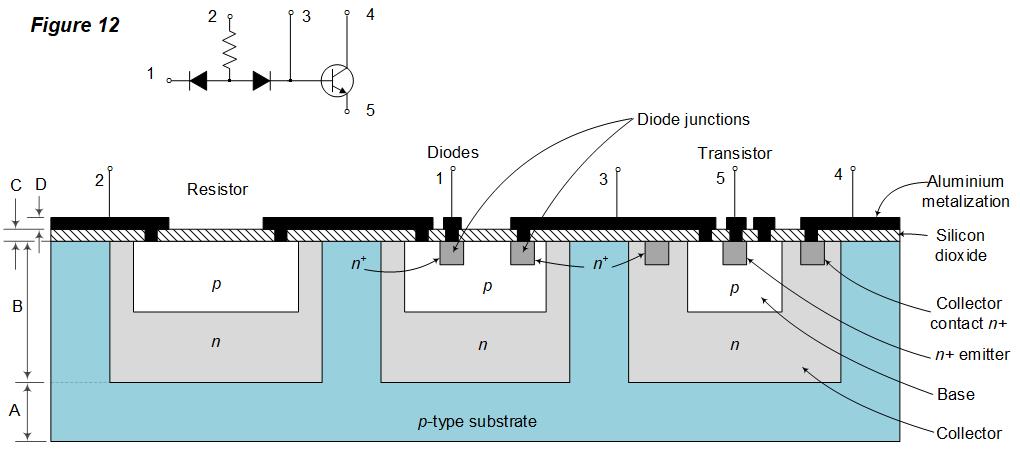
In the regions where diffusion is to take place, the SiO2
layer is etched away, leaving the rest of the wafer protected against
diffusion.
To permit selective etching, the SiO2
layer must be subjected to a photolithographic process that will be
discussed later on.
Finally, a fourth metallic (aluminum) layer (D) is added to supply the
necessary interconnections between components.
In our IC example, the circuit consisted, as the above figure shows,
of a resistor, two diodes and a transistor and five connection wires.
The above described IC configuration is called a monolithic integrated
circuit because it is formed on a single silicon chip. The word
"monolithic" is derived from the Greek word "monos"
meaning "single" and "lithos" meaning
"stone".
3.8.2. IC Process description
In this chapter, the processes are discussed which are required to
fabricate IC's.
Figure 13a through 13e can be consulted to get a better view on the
individual processes.
3.8.2.1 Substrate fabrication process
A tiny crystal of silicon is attached to a rod and lowered into a
crucible of molten silicon to which p-type acceptor impurities have
been added.
As the rod is very slowly pulled out of the melt under carefully
controlled conditions, a single p-type crystal ingot is grown. The
ingot is subsequently sliced into round wafers to form the substrate
upon which all integrated components will be fabricated.
One side of each wafer is lapped and polished to eliminate surface
imperfections before proceeding to the next process.
3.8.2.2 Epitaxial growth process (see figure 13a)
An n-type epitaxial layer, typically 15μm thick, is grown into a
p-type substrate using the epitaxial growth process. This epitaxial
process consist of the following process steps:
A precise defined mixture of a reactive gas and a
layer of concentrated inert gas is, with a precise controlled speed and at a
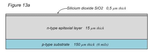 temperature of
1200°C, inserted in a reaction chamber where the gas flows over
the surface of the substrate. The gas mixture does not only contain the required n-type doping
material but also contains for that purpose an appropriate silicon
compound such as silicon tetrachloride (SiCl4). The reactive in the gas evokes a chemical reaction on the surface of
the substrate and the silicon will continue to grow using the silicon
atoms and doping atoms from the gas mixture. temperature of
1200°C, inserted in a reaction chamber where the gas flows over
the surface of the substrate. The gas mixture does not only contain the required n-type doping
material but also contains for that purpose an appropriate silicon
compound such as silicon tetrachloride (SiCl4). The reactive in the gas evokes a chemical reaction on the surface of
the substrate and the silicon will continue to grow using the silicon
atoms and doping atoms from the gas mixture.
The basic chemical reaction used to describe the epitaxial growth of
pure silicon is the hydrogen reduction of silicon tetrachloride: SiCl4 + 2H2
<==> Si + 4HCl
After the silicon grow process has been completed, the by-products of the chemical reaction
are removed from the reaction chamber. After polishing and cleaning, a
thin layer (0.5μm) of silicon oxide (SiO2), is formed
over the entire wafer as can be seen in figure 13a.
The SiO2 layer is grown by exposing the epitaxial layer to
a steam atmosphere while being heated to about 1000°C. Silicon
dioxide has the fundamental property of preventing the diffusion
of impurities through the silico dioxide. This property is used in
the following process steps.
3.8.2.3 Isolation diffusion (see figure 13b)
In figure 13b the wafer is shown with the SiO2 layer
removed in four different places on the surface. This removal is
accomplished by means of a photolithographic etching process before
the actual diffusion takes place.
The remaining SiO2 material serves as a mask for the
diffusion of p-type impurities.
The selective removal of
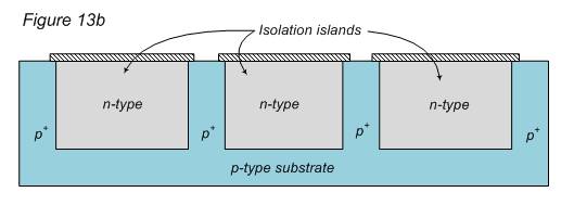 the SiO2 layer can best be compared with the removal of
copper on a printed circuit board using an etching process. the SiO2 layer can best be compared with the removal of
copper on a printed circuit board using an etching process.
The total area of the wafer is coated with a uniform film of a
photosensitive emulsion.
A large black-and-white layout of the desired pattern of openings in
the SiO2 is made end then reduced photographically.
This negative, or stencil, of the required dimensions is placed as a
mask over the photoresist.
By exposing the photoresist to ultraviolet light through the mask, the
photoresist becomes polymerized under the transparent regions of the
stencil.
Remark: Nowadays, the structures on a chip are that small that
it is obvious that exposing by ultraviolet light is not possible
anymore simply due to the fact that the dimensions of the structures
on the chip approach the wavelength of the employed light. This will
lead to resolution problems.
In case of dimensions in the sub-micron area, the quite expensive
X-ray lithography process is yet still in use. An alternative solution
is to make use of the electron beam lithography process that even
enables direct writing on the chip.
Quite new developments are ongoing in the area of laser lithography
whereby even resolutions in the order of 10 nanometer can be achieved.
The mask in now removed, and the wafer is developed by using a
chemical substance which dissolves the unexposed (unpolymerized)
portions of the photoresist film. The emulsion which was not removed
in the development process is now fixed, or cured, so that it becomes
resistant to the corrosive etches used in the next process.
The chip is now immersed in an etching solution which removes the SiO2
from the areas where the emulsion has been removed and through which
dopants are to be diffused.
After diffusion of impurities, the polymerized resist mask is removed
with a chemical solvent coupled with a mechanical abrasion process.
The most important process in IC fabrication is the diffusion process
which takes place at a temperature of 1000°C. With respect to the
reproducibility of the diffusion process, this temperature must be
maintained within 1-2°C.
A mixture of metal vapor which contains the p-type impurities and an
inert gas, for instance nitrogen, brings the impurity atoms to the
surface of the wafer where they can diffuse into the n-type epitaxial
layer until they reach the p-type substrate.
In that way we obtain the three gray shaded n-type isolation regions as can
be seen in figure 13b.
These sections are called isolation islands because they are separated
by two back-to-back p-n junctions. Their purpose is to allow
electrical isolation between different circuit components.
The p-type substrate must always be held at a negative potential with
respect to the isolation islands in order that the p-n junctions be
reversed biased. If these diodes were to become forward biased in an
operating circuit, the isolation would be lost.
It should be noted that the concentration of acceptor atoms in the
region between isolation islands will generally be much higher than in
the p-type substrate. These region are therefore indicated by a p+.
The reason for this higher concentration is to prevent the depletion
region of the reverse biased isolation-to-substrate junction from
extending into the p+-type material and possibly connecting
two isolation islands.
A more advanced technique that also facilitates very accurate doping
is the so called ion-implantation. From the point of view of process
technology, the characteristic of ion-implantation is that it is a
cold process, this in contrast with the above described diffusion
process which takes place at a temperature of 1000°C.
This advantage combined with the possibility to define very well the
profile of the doping, makes that this technique is preferably used in
the fabrication of modern high quality integrated circuits.
In ion-implantation, the wafer is placed in an evacuated chamber and
bombarded with accelerated ionized atoms of the
required doping material. By adjusting the energy of the ions, the
penetration depth can precisely be determined.
Ion-implantation is a very expensive technique, however, for the
fabrication of MOS circuits it is indispensable. MOS stands for
"Metal Oxide Semiconductor". These MOS components will
be discussed later on very briefly, this because they have specific
advantages over transistors and hence are quite often employed in
digital circuits such as controllers, micro-processors and memory
devices.
3.8.2.4 Base diffusion
During this process a new SiO2 layer is formed over the
wafer, and the photolithographic process is used again to create the
pattern of openings shown in figure 13c.
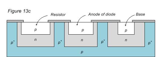 The
p-type impurities are diffused through these openings and, in this
way, the transistor base regions as well as the resistors and the
anode of diodes are formed. The
p-type impurities are diffused through these openings and, in this
way, the transistor base regions as well as the resistors and the
anode of diodes are formed.
It is very important to control the depth of the diffusion so that it
is shallow and does not penetrate to the substrate.
3.8.2.5 Emitter diffusion
A layer of SiO2 is again formed over the entire surface of
the wafer and the masking and etching processes are used again to open
five windows in the p-type regions as shown in figure 13d.
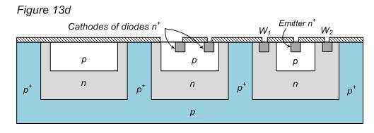 Through
these openings n-type impurities are diffused for the formation of the
transistor emitters and the cathode regions for the diodes. Through
these openings n-type impurities are diffused for the formation of the
transistor emitters and the cathode regions for the diodes.
Additional windows, such as W1 and W2 in figure 13d, are often made
into the n-regions to which a lead is to be connected for making
interconnections.
During the diffusion of phosphorus in this case, a heavy concentration n+
is formed at the points where contact with aluminum is to be
made. Aluminum is a p-type impurity in silicon, and a large
concentration of phosphorus prevents the formation of a p-n junction
when the aluminum is alloyed to form an ohmic contact.
3.8.2.6 Aluminum metallization
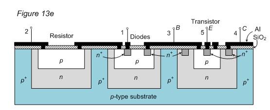 All
p-n junctions and resistors have been formed in the preceding process
steps. It is now necessary to interconnect the various components of
the IC as dictated by the electronic circuit. All
p-n junctions and resistors have been formed in the preceding process
steps. It is now necessary to interconnect the various components of
the IC as dictated by the electronic circuit.
To make these connections, a set of windows is opened for the fourth
time into a
newly formed SiO2
layer at the points where contact is to be made.
The interconnections are made using vacuum deposition of a thin coating of aluminum over the entire wafer. The photoresist
technique is now applied to etch away all undesired aluminum areas,
leaving the desired pattern of interconnections between resistors,
diodes and transistors (see figure 13e).
After the metalization process has been completed, the wafer is scribed
with a diamond-tipped tool and separated into the individual chips.
An example of a complete wafer can be seen in the picture below while
the extraction shows an
enlarged part of a single chip on the
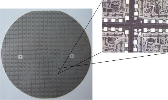 wafer. One
can clearly see the square wafer. One
can clearly see the square
pads where the bonding wires are to
be connected and the black separation lines of the individual chips.
Furthermore, this
chip-picture shows a more complex chip that very likely concerns a microprocessor chip
from back in 1980. The quite uniform areas in the center of the chip are memory cells of
the processor (RAM and ROM).
3.9 Field-effect transistors
A field-effect transistor is a semiconductor device which
depends for its operation on the control of current by an electric
field. Because the conduction of current predominantly takes place
by majority carriers, these devices are called unipolar transistors.
There are two types of field-effect transistors, the junction
field-effect transistor (abbreviated JFET, or simply FET) and the
metal-oxide-semiconductor field-effect transistor (abbreviated
MOSFET).
Both types will be discussed briefly this in order to complete the
total transistor picture.
Another reason to discus them is the fact that field-effect
transistors have remarkable advantages over bipolar transistors.
These advantages are:
1) The operation of field-effect transistors depends upon the flow
of majority carriers only and
therefore a lot of parameters are less
sensitive to temperature changes.
2) Field-effect transistors are simpler to fabricate and circuits
occupy less space in integrated
form.
3) High input impedance in the order of 1010 Ω.
4) Field-effect transistors can be used as a symmetrical bilateral
switch.
5) By means of the charge stored on small internal capacitances, the
field-effect transistor
functions as a memory device.
3.9.1 The JFET
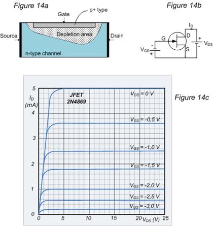
The structure of an n-channel field-effect transistor is shown
in figure 14a. Ohmic contacts are made to the two ends of a
semiconductor bar of n-type material.
On top of the bar, a layer of p-type material is diffused which is
provided by an ohmic contact as well.
In case of a p-channel JFET the type of p and n-material is just
opposite.
We will only discuss here the n-channel JFET.
If we connect a voltage supply between the two ends of the n-channel
bar (see figure 14b), current is caused to flow. This current
consists of majority carriers, which in this case are electrons. The
terminal through which the majority carriers enter the bar is called
the source and where they leave the bar is called the drain.
The p-type layer that has been diffused on top of the n-type bar is
called the gate.
As we saw earlier at the bipolar transistor, that around a p-n
junction, a depletion area is formed of which the depth of the area
depends on the voltage applied across the p-n junction.
Furthermore, we have learned that this layer predominantly extends
to the less doped area.
Because the gate layer is heavily doped (p+), the
depletion region will extend deep into the n-channel area.
In normal use, the junction between the channel and the gate is
reverse biased (see figure 14b).
Let's now consider the conductivity of the channel in the direction
of source to drain.
The depletion layer is depleted of mobile charge
carriers which in fact implies that the available material for
conductivity is only n-type material outside the depletion region.
An increase of reverse bias of the gate-source will increase the
depletion region and hence conductivity decreases. On the other
hand, decreasing the reverse bias will increase conductivity. Thus
it is possible to control the current between source and drain by
means of the gate voltage. The voltage VDS
applied between drain and source causes the junction
voltage at the location of the drain to be greater than the voltage
at the location of the source. In other words the drain end of the
gate is more reverse biased than the source end, and hence the
boundary of depletion is not parallel to the longitudinal axis of
the channel but is curved as shown in figure 14a.
At a specific combination of VGS and VDS, the
depletion layer at the location of the drain will extend to the full
depth of the n-channel causing the current flow to be zero.
This is called
"pinch-off". The voltage VGS , at which at a
given value of VDS pinch-off occurs, is called
pinch-off voltage.
When VDS increases, current will rapidly increase until
the saturation current is reached.
Figure 14c shows the characteristic of a n-channel JFET.
3.9.1.1 Fabrication of the JFET
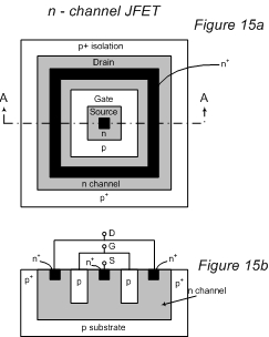
Figure 15a shows the top view geometry of a JFET while figure 15b
shows the cross section in the plane AA.
The substrate is of p-type material onto which an n-type channel is
epitaxially grown. A p-type gate is then diffused into the n-type
channel. The p-type gate is heavily doped (p+) to allow the
depletion layer to penetrate into the n-type channel.
3.9.2 De MOSFET
In a junction field-effect transistor (JFET) an electric field is
applied to the channel through a p-n diode. A basically different
field-effect device is obtained by using a metal gate electrode
separated by an oxide layer from the semiconductor channel.
By applying an external voltage between the gate and the substrate,
the electric field will influence the channel.
Such a device is called a MOSFET or MOS transistor and is of much
greater importance than the JFET because it can be fabricated much
smaller than the JFET which gives the advantage of less current
consumption and operation at much higher frequencies. This is very
important in today's generation microprocessors and memory devices.
There are two types of MOSFETs, the "depletion"
MOSFET and the "enhancement" MOSFET.
Both types can exist in either the p-channel or an n-channel variety.
Therefore, four types of
MOSFET transistors can be distinguished as the picture below
indicates.
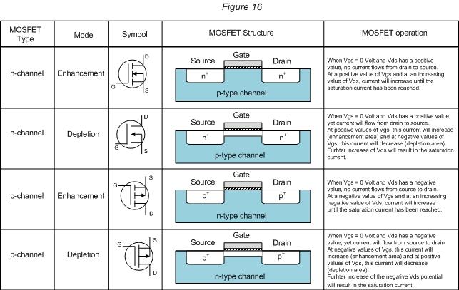
Notice that in the n-channel and p-channel MOSFET, the p+
and n+ regions are fully isolated, this in contrast with
the n and p-channel depletion MOSFET. In the depletion devices, the
drain and source are connected through a small diffused layer of the
same type of impurities as used for the drain and source.
This means that at VGS is 0 Volt, yet a current will flow
from drain to source.
As far as the operation and fabrication is concerned, only the n-channel enhancement
MOSFET will be discussed, this to keep it simple.
3.9.2.1 The n-channel enhancement MOSFET
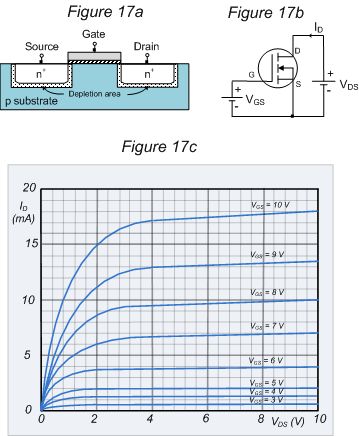
At equilibrium, when no voltages are connected to the MOSFET, the
p-substrate and n+ source and drain form a p-n junction.
Therefore a depletion region exists between the n+ source and drain
and the p-substrate as can be seen in figure 17a on the right.
Since the source and drain are separated by back-to-back p-n
junctions, the resistance between the source and drain is very high
(approximately 1012 Ω.
When a positive potential is applied to the gate with respect to the
source (see figure 17b) and no voltage is applied yet between drain
and source, holes located under the gate will extend deeper into the
p-substrate while for the electrons the opposite is valid. Right under
the gate, a thin layer is formed in which only electrons are available
as charge carriers.
This situation is called "inversion" since the layer has now
obtained the characteristics of n-material. Such an inversion layer,
and thus a significant conductive channel, is formed only if the gate
voltage exceeds the so called threshold voltage.
When a voltage is now applied between drain and source (see figure
17b), drain current ID will start to flow provided VGS
extends the threshold voltage.
Now, it is also clear where the term enhancement MOSFET comes from.
When VGS = 0 Volt, no drain current will flow. Values of VGS greater
than zero volt will enrich (enhance) the channel this in contrast with
the
depletion type MOSFET where certainly flows a drain current when VGS = 0 Volt.
By making VGS negative, the channel will reduce to
poverty (depletion) or even the channel is made completely empty.
Figure 17c shows the ID-VDS characteristic of an
n-channel enhancement MOSFET with VGS as parameter.
3.9.2.2 Fabrication of an n-channel enhancement MOSFET
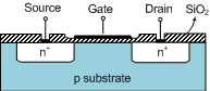 Starting
with a p-type substrate, a SiO2 layer is grown on the
surface. Using the standard masking and etching processes, two
openings are made in the SiO2 layer through which n-type
impurities are diffused for making the source and drain region. Starting
with a p-type substrate, a SiO2 layer is grown on the
surface. Using the standard masking and etching processes, two
openings are made in the SiO2 layer through which n-type
impurities are diffused for making the source and drain region.
A thick layer of oxide is grown over the surface and a second masking
and etching process results in three openings in the SiO2
(see figure on the right). In the middle opening, a thin layer of SiO2
is added for the gate oxide. A third mask allows the oxide covering
the source and drain regions to be etched away. Aluminum is then
evaporated over the entire surface and a final masking and etching
process removes the undesired aluminum so as to remove the
interconnections between source, gate and drain and leaves the source,
gate and drain connection intact.
The term "metal" in the name Metal Oxide
Semiconductor FET, is presently somewhat misplaced. In the early
days, the gate material was indeed aluminum but nowadays this material
is polysilicon (crystalized pure silicon).
The reason for this change is that polysilicon offers the possibility
to fabricate so called
"self-aligned" gates. In the conventional fabrication of a
metal-gate MOS an additional photomasking step is necessary to
align the gate with the source and drain which have already be formed.
An overlap of 0.2 mil is necessary to ensure that the gate extends
from the source to the drain regions. This overlap increases the
capacitance between gate and source and also between gate and drain.
These capacitances lower the speed of operation and increase power
consumption.
The so called "self-aligned" MOSFET structure can prevent
this problem.
The idea of the
"self-aligned" MOSFET encompasses the use of a pre-defined
gate which is used as a mask for the diffusion steps. Thus, the gate
is already formed before the diffusion of the source and drain takes
place, following that, the same mask is used for the diffusion of the
source and drain.
The big challenge to use the "self-aligned" structure is the
choice of the gate material. To determine this material we first have
to look what doping techniques are available. These are diffusion and
ion implantation.
Diffusion requires a temperature of 1000°C. Although ion
implantation can take place at a much lower temperature
(200°C), crystal damages that are caused by the high energy
ions have yet to be repaired by using an annealing process which takes
place at a temperature of 800°C.
The in the early days (1970-1980) used gate material aluminum will
however, at a temperature of 500°C, diffuse into the gate oxide
material so one had to search for another gate material.
It appeared now that doped polysilicon was the best choice of material
for the gate since it could withstand the high anneal temperature and,
moreover, oxidation was as easy as silicon.
Note that the doping of polysilicon is done to increase conductivity.
3.9.3 Complementary MOSFET
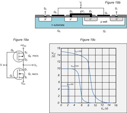 It
is possible to construct p-channel and an n-channel enhancement MOSFET
devices on the same chip. Such devices are called Complementary MOSFETs
better known as CMOS devices. It
is possible to construct p-channel and an n-channel enhancement MOSFET
devices on the same chip. Such devices are called Complementary MOSFETs
better known as CMOS devices.
The schematic representation of a CMOS device is shown in figure 18a
on the right. As can be seen, the circuit consists of a p-channel
MOSFET and an n-channel MOSFET which are internally interconnected in
such a way that drain D1 is connected to drain D2.
The gates G1 and G2 are also internally connected.
The G1-G2 connection is now connected to an external input voltage Vi
while the D1-D2 connection is supposed to be the output terminal Vo.
The input voltage can be between 0V en +VDD. When Vi = 0V
then Q1 will be blocked because VGS1
= 0 Volt. However, Q2 will be fully conducting because VGS2
is equal to -VDD.
Because VDS2 = 0V, the output voltage Vo is equal to
+VDD.
In case the input voltage Vi is equal to +VDD , VGS1
will also be equal to +VDD
causing Q1 to be fully conducting. Because VGS2 is now
equal to 0 Volt, Q2 will be blocked and hence the output voltage Vo
will be 0 Volt.
From the above we can state that the described CMOS device behaves
like an inverter.
Figure 18c shows the transfer characteristics of this inverter at
three different supply voltages +VDD i.e. 5, 10 and 15Volt.
3.9.3.1 Fabrication of a CMOS inverter
The fabrication process starts with an n-type substrate into which
a p-type "well" or "tub" is diffused. The NMOS
transistor Q1 is formed in this p-type well and the PMOS transistor Q2
in the n-type substrate. Figure 18b above shows a simplified
structure of this CMOS device.
In reality, this structure is quite different then the simplified
version shows, this to prevent "latch-up" at any time.
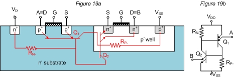 Latch-up
is a state or condition in which the p-MOSFET and the n-MOSFET
are both conducting. Latch-up
is a state or condition in which the p-MOSFET and the n-MOSFET
are both conducting.
This means in most cases a complete burn-out of the chip.
The question is now, how can such latch-up situation occur?
To answer this question we take a look at figure 19a in which we have
drawn two red colored stray or parasitic transistors Q1 and Q2. We
obviously see that the different p and n regions in the CMOS device
create the possibility of forming parasitic transistors.
The emitter of transistor Q1 could be p+
area of the p-MOSFET while the basis of Q1 could be formed by the n-
substrate. The collector of Q1 is represented by the p-well.
An identical configuration can be set-up for transistor Q2. The n+
regions of the n-MOSFET form the emitter of Q2 while the basis of Q2
is formed by the p-well. Finally, the collector of Q2 is formed by the n-
substrate.
The resistor RN- is the resistance from the base of Q1 and
the collector of Q2 to VDD . The resistor RP- is
the resistance from the collector of Q1 and the base of Q2 to VSS
.
This complete parasitic circuit has been schematically represented by
figure 19b. In this circuit we can clearly see that latch-up can occur
when a voltage spike is injected to VDD or node A.
Application of this voltage spike cause a very small leakage current
to flow through the collector of Q1 which in turn produces a base
current for transistor Q2.
This base current will turn on Q2 even more and thus increases the
base current for Q1 which will also turn on.
This regenerative process will eventually lead to a full short between VDD
and VSS with the consequence that that the CMOS
device will completely be destroyed.
To prevent this latch-up situation, various precautions can be taken.
One approach is to keep the source-drain of the p-channel device as
far away from the p-well as possible.
This reduces the β of transistor Q1 and helps to prevent latch-up.
Unfortunately, this is very costly in terms of chip area.
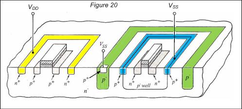 A
second approach is to reduce the resistor values of RN-
en RP-. Smaller resistor values are helpful because more
current has to flow through them in order to forward bias the
base-emitter regions of Q1 and Q2. A
second approach is to reduce the resistor values of RN-
en RP-. Smaller resistor values are helpful because more
current has to flow through them in order to forward bias the
base-emitter regions of Q1 and Q2.
These resistances can be reduced by surrounding the p-channel devices
with a so called n+
guard ring that is connected to VDD and by diffusing a p+ guard ring
into the perimeter of the p-well that is connected to VSS
.
A third approach is to make a deep p- diffusion guard ring
outside of the p-well which is connected to VSS. This will
short the collector of Q1 to VSS and hence, cannot deliver
base current to Q2.
The principle of applying guard rings is depicted
in figure 20.
Another important consideration of CMOS technology is the
electrostatic discharge protection of the gates of transistors which
are externally accessible. Static electricity may vary from 2 kVolt to
even more than 10 kVolt, depending on the circumstances.
When a CMOS gate comes in direct contact with such a voltage, for
instance by touching the leads of an IC, the gate oxide will be
damaged instantly.
To prevent accidental destruction of the gate oxide, a resistance and
two reverse biased p-n junction diodes are employed to form an input
protection circuit.
Nevertheless, caution must still be taken when working with CMOS devices.
An earthed wrist strap and use of conductive foam or conductive
plastic bags in case of packaging material is to be used, is no
superfluous luxury
3.10 The future of the chip
(Ref. Technisch Weekblad Februari 2008)
If we take a look at the development of the transistor from the moment
of its invention in 1947 till today, we must state that the
transistor, and all its derivatives, has gone through en enormous
development scenario.
Gordon Moore, co-founder of the Intel chip manufacturer, wrote in 1965
nothing of particular importance when he stated that the complexity of
integrated circuits was doubled each two years at minimum cost and
that there was no reason to assume that this would change in the next
decennium.
Today, everybody knows Moore's law as a proposition that the math
power of microprocessors doubles each two years. The law has hold
perfectly the last 40 years though it has changed the last years from
a prophecy into a business objective for chip manufacturers.
The table below gives an impression of chip development where a remark
is to be made that wafer size has increased
drastically from 19 mm in
1959 to 300 mm in 2007.
It is quite conceivable that that this enormous density
of transistors poses extreme high requirements on the equipment to
fabricate the chip, the waferstepper.
A modern waferstepper operates simply spoken as follows: The first
step is to apply a layer of photosensitive material i.e. photoresist
to a thin wafer of pure silicon which can be as large as 12 inches (300 mm) in
diameter.
By using a mask that contains the complete lay-out of the chip and by using an
optical system that reduces the image on the mask, a laser beam will
expose the photoresist layer which will thus takes a copy of the
pattern of transistors on the mask.
Subsequently the waferstepper moves to the wafer in order to repeat
the process until the whole wafer is covered with identical chips.
After forming the different layers and intermediate diffusion steps,
the wafer is ready to be scribed and separated into individual
micro-chips.
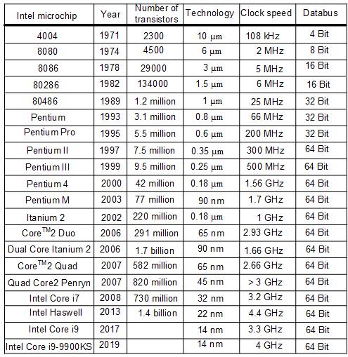
Chapter 4 Development of electronic components
and their packaging
In the next and last chapter, a photo-session and brief descriptions
will be presented to aid in depicting the development of the various
electronic components and their packaging during the past decennia.
Parts where no text and explanation is given do speak for themselves.
1 Electron tubes
It is apparent that we start-off with a collection of old electron
tubes.
On the far left we see a transmitting tube that was used in a so
called vein eraser that was used to clean varicose veins by employing
high frequency energy.
Note that the dimensions of the tubes have drastically decreased over
the past years.
2 Resistors
This picture shows an extensive collection of resistors. On the far
left you see an ancient carbon resistor mounted in an hermetically
sealed glass housing.
On the far right you see the today used Surface Mount Devices (SMD)
resistors.
Not shown are for instance resistor types such as NTC resistors, VDR
resistors, wire wound resistors and variable resistors.
3 Capacitors
This collection of resistors is just a small sample from a very large
variety of capacitors.
The three capacitors on the left, next to the gray tubular Philips
capacitor, are SMD capacitors.
If you look carefully you will see on the top left that the brownish
ceramic capacitor has got the capacitance value indicated in cm (1 cm
equals 0.9 pF). Unfortunately, the text on the capacitor is upside
down.
4 Electrolytic capacitors
This picture shows a collection of capacitors ranging from an old
electrolytic capacitor on the far left to SMD capacitors on the lower
right.
5 Coils
6 Rectifiers
7 Relays
8 Light Emitting Diodes (LED)
9 Displays
On the upper left you see a 7-segment display including the segment
driver. In the middle you see the well known old nixie tubes from Hewlett Packard
and Siemens.
On the right you see some nice examples of the so called VFD (Vacuum
Fluorescent Display) displays. These types of display are mainly
used in video recorders, DVD recorders, microwave ovens etc. because
of their superior brightness and contrast.
10 Crystals
11 Transistors
12 TV Picture tube Electron guns
In this picture we can see the development in television picture tubes
and in particular the electron guns. On the far left side we see the
classical triangular set-up of the RGB electron guns. Unfortunately,
this set-up of the electron guns caused severe converging problems in the formation of the
picture. In order to strongly reduce that problem the electron guns
were lined-up horizontally which is clearly shown in the picture on
the right.
13 Digital and Linear Integrated Circuits
This picture shows just a very small collection of the enormous
variety in digital and linear integrated circuits. Notice the
difference in assembly techniques.
Usually, most integrated circuits are intended for commercial use and
therefore have the "commercial grade" classification and are
encapsulated in plastic. However, in applications that demand high
requirements on reliability of the integrated circuit, the devices are
mounted in a ceramic packaging. For instance look at op-amp IC LM324 and D/A converter DAC90.
14 Hybrid circuits
This picture shows a summary of various hybrid circuits. On the
left we see an implementation of early hybrid technology
in the so called Philips "circuit blocks" in which the
components were mounted on a printed circuit board and encapsulated
in silicone rubber or epoxy.
If we click on this picture,
we will see a close-up of the circuit blocks.
Nowadays, all components are usually mounted on a substrate of
aluminum oxide.
By clicking on this picture, we see
a nice close-up of an isolation amplifier hybrid and a DC/DC
converter hybrid that even contains a transformer mounted on the
substrate.
On the right of this close-up we see some hybrids that were used in
implantable pacemakers. Note that the seam welded lids of the
hybrids have been removed.
This pacemaker hybrid is a hybrid that was used in the very first dual chamber
pacemaker of Medtronic. The pacemaker was a so called ASVIP
pacemaker. ASVIP stands for Atrial
Sequential
Ventricular Inhibited Pacemaker.
This pacemaker system, that includes two electrodes which are
introduced into the heart, is capable of detecting the rhythm of the
atrium and the ventricle.
The very same electrodes are used to stimulate the atrium or the
ventricle, or even both.
In a healthy cardiac system, the rhythm of the atrium is determined
by the so called SA
node (sinoatrial node). The SA node triggers the atrial muscle that
contracts (depolarization). Via the muscle fibers of the atrium, the
impuls is then conducted to the AV node (atrioventricular node). It is important to note that the impulse will reach the AV node after a delay of 100-150 ms, this to enable a
controlled contraction of the atrium and to give the ventricle the
opportunity and time to fill with blood.
AV node triggering evokes another impulse that is further conducted,
via the bundle of His, to the ventricle which will contract
(depolarization).
After all cells of the muscle have repolarized, the cycle starts
again.
In case of an AV block, conduction to the ventricle is obstructed
and the pacemaker will detect this deficiency causing the
pacemaker's ventricular output circuit to stimulate the ventricle
after a certain delay period.
In case no signal from the SA node would be detected by the
pacemaker, the atrium will be stimulated by the pacemaker's atrial
output circuit. The atrium contracts and after normal conduction to
the AV node and normal conduction delay through the bundle of His,
the ventricle will contract.
It is worthwhile to mention that all parameters of the pacemaker
could be programmed by an external programmer via RF telemetry.
Parameters such as atrial and ventricular stimulation and sensing
parameters, A-V delay and refractory time after
atrial or ventricular stimulation could be programmed.
15 Chip carriers
This picture shows how the individual integrated circuit is mounted
in its package which is called the chip carrier.
If we click on this close-up
picture of a chip carrier, we clearly can see the wire bonding.
Unfortunately, some of the wires have been destroyed during removal
of the lid of the carrier.
16 Single chip microprocessors
On this picture you will see two microprocessors that contain a
small circular glass window. These microprocessors are called EPROM
microcomputers in which application programs can be loaded.
Such an application program contains a series of instructions stored
in program memory within the microcomputer.
The processor in the microcomputer fetches these instructions one at
a time and executes the operation indicated.
The application program can be erased by subjecting the chip to
ultraviolet light through the glass window. A new application
program or an update of an existing program can then be programmed and used again
for an other application.
17 Microprocessor Peripheral Devices
18 PC Microprocessor and Controllers
Further development of the components shown on the picture in paragraph
16 and 17 has ultimately resulted in the realization of the
first processors and controllers used in early personal computers
(PC).
If we click on this picture, we
will see the Pentium MMX chipset.
This picture shows the Pentium4
chipset and the AMD Athlon
A0850 processor.
19
4
kByte magnetic core memory
This old magnetic core memory card contains only 4kBytes of memory and has a
dimension of 28x42 cm.
For fun, compare these dimensions with a 2 Gbyte memory bank card in a
modern PC.
Here you can see a detailed view
of the magnetic cores.
20 RAM memory
21 EPROM memory
22 Data retention media
23 Hard disks
Note:
This collection of radios, including the components that did play an
important role in the development of electronics, have been stored on
my loft and can be identified as a kind of museum.
A short impression of this "museum" is given by the pictures
below.
Click on the pictures to show them enlarged in a new window.
In case you have suggestions or questions, do not
hesitate to send an e-mail to the
webmaster
|
|
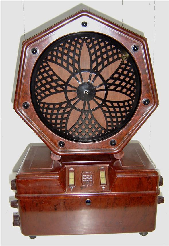
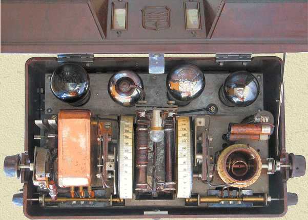
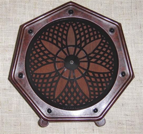

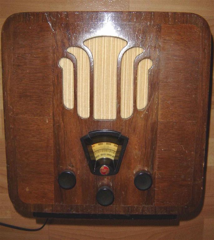
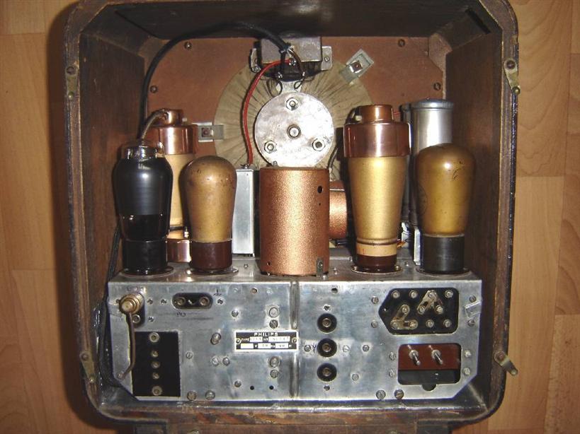
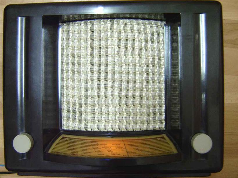
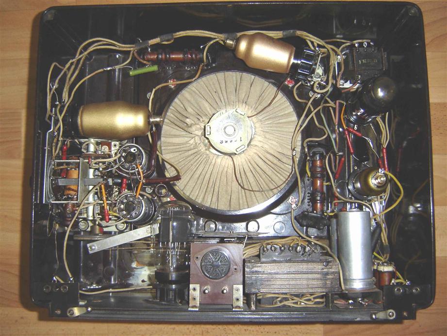
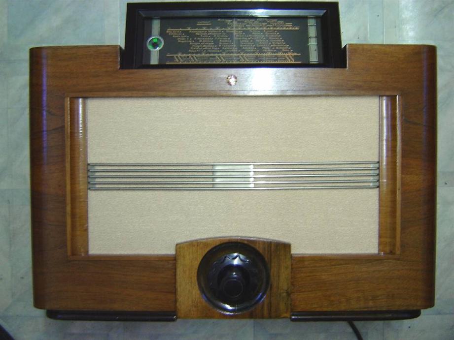
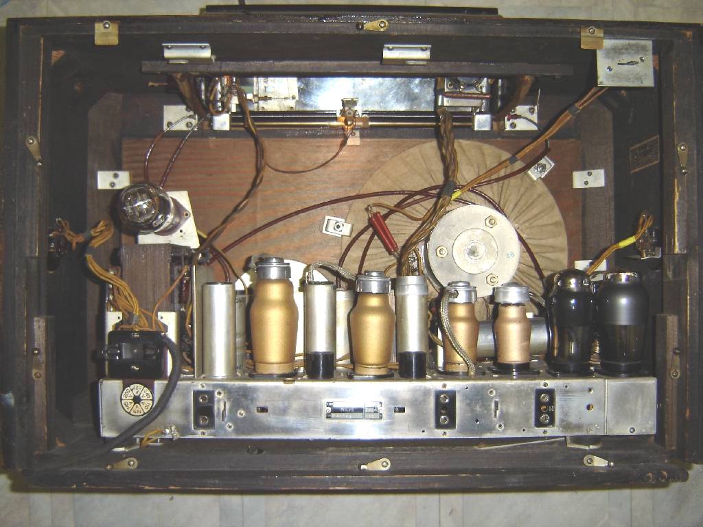
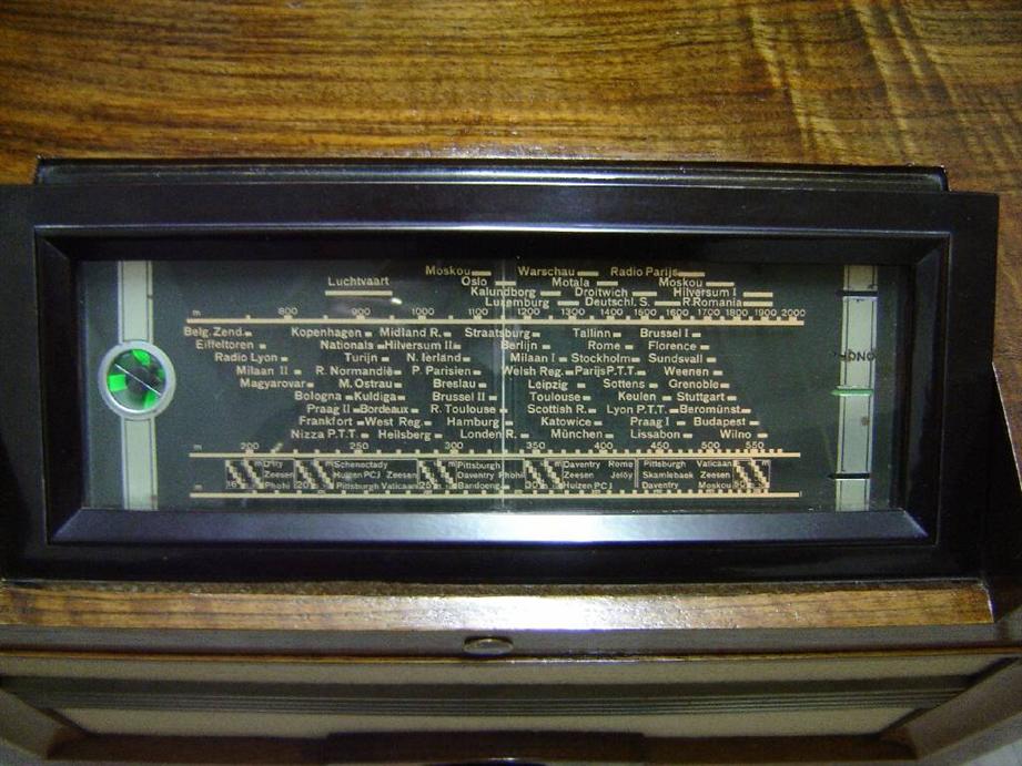
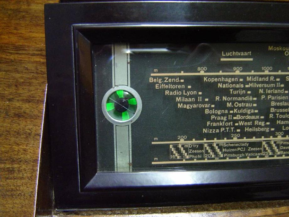


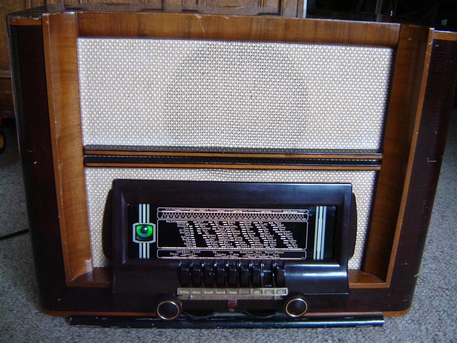

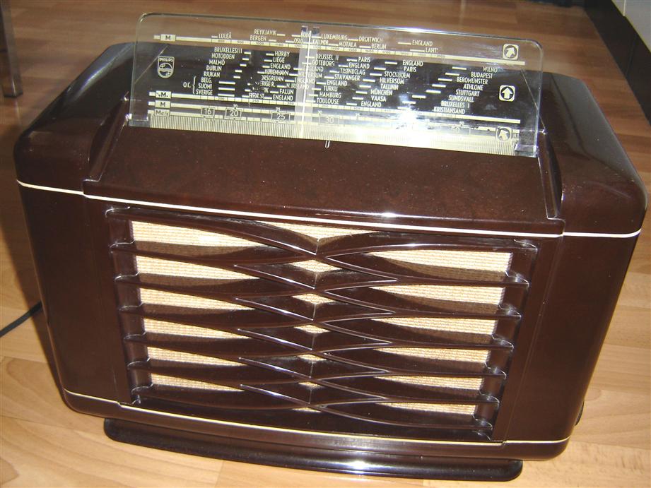
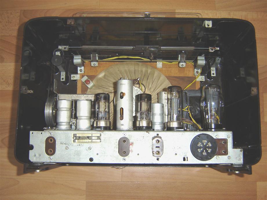
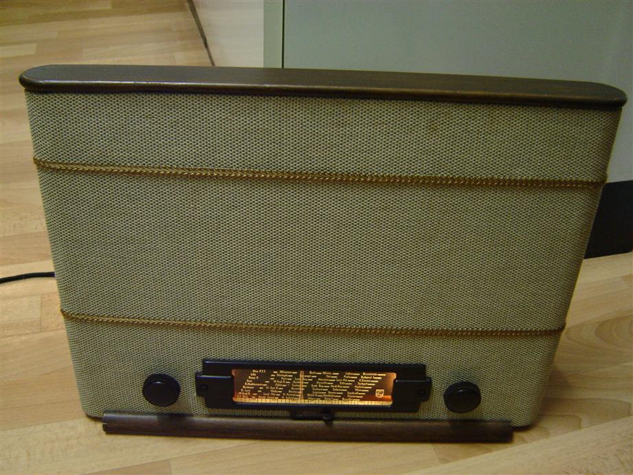
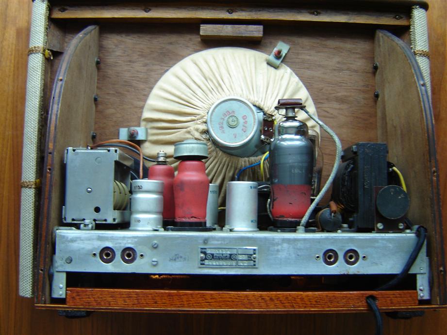
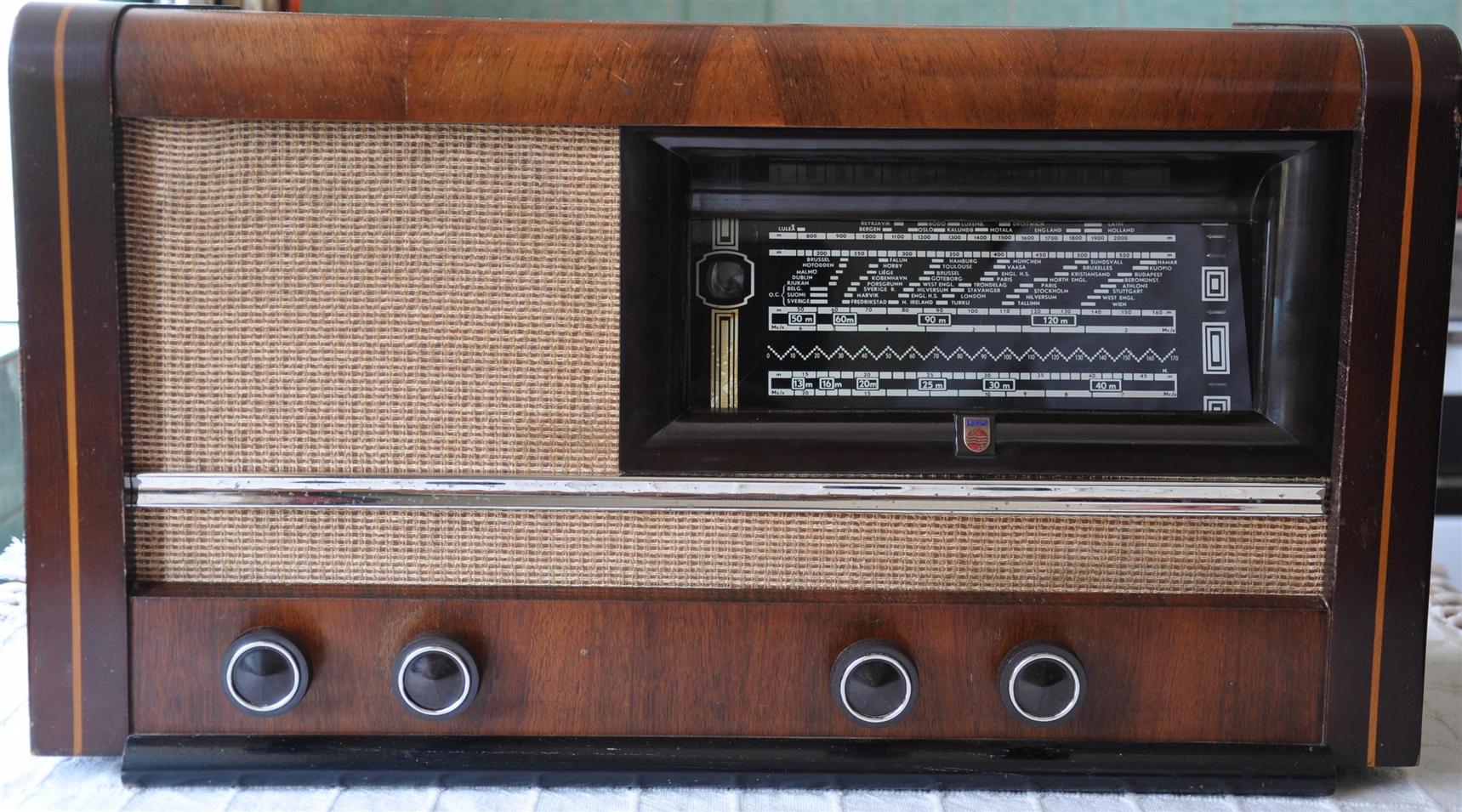
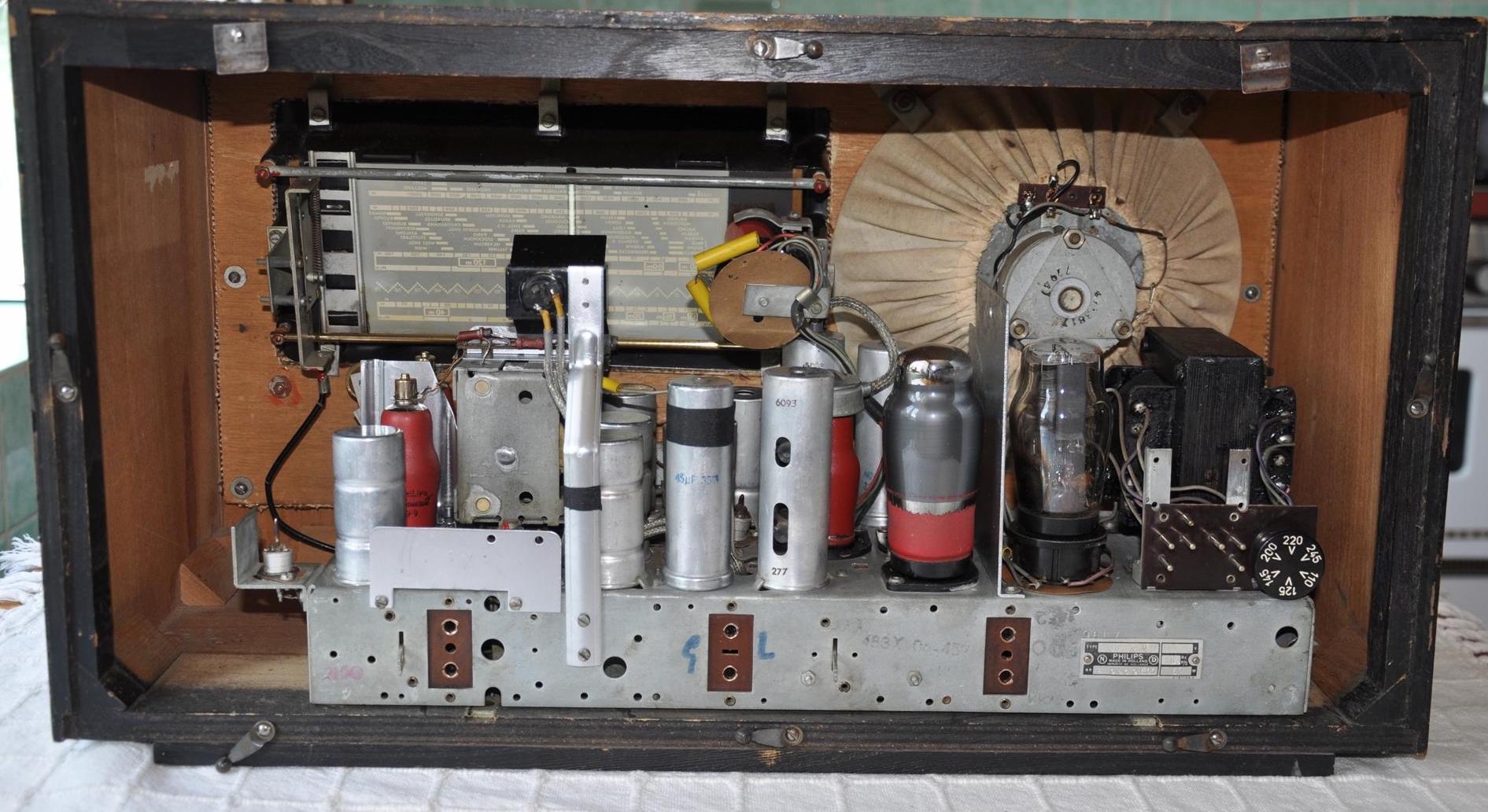


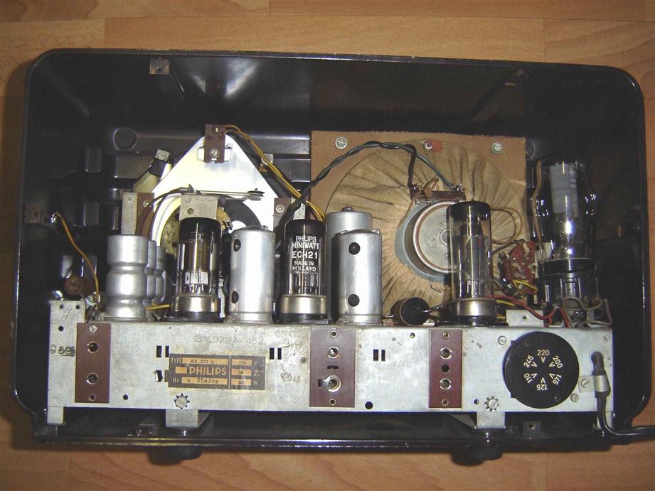
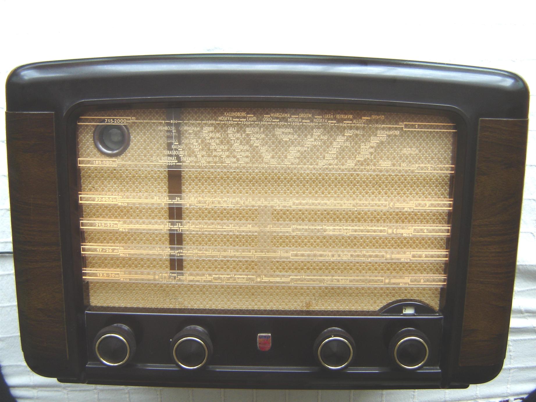
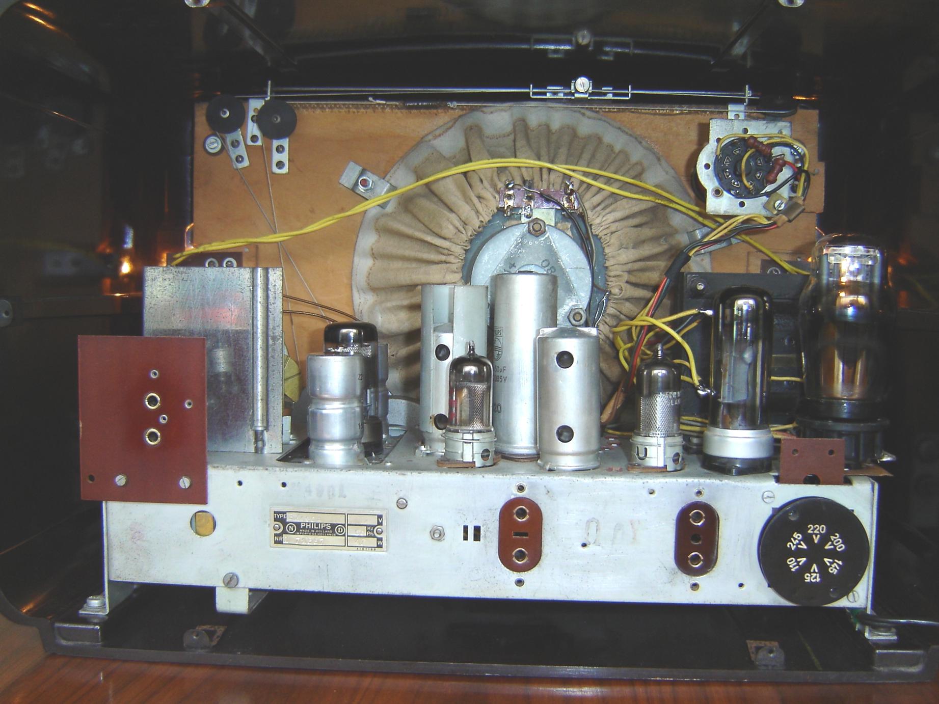
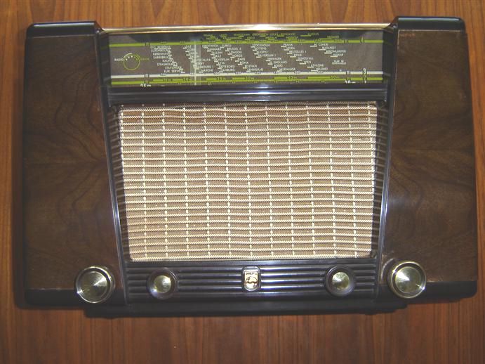
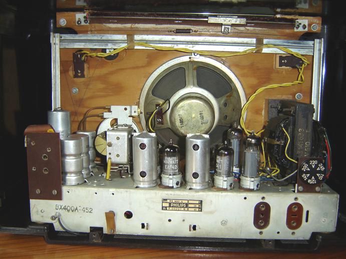
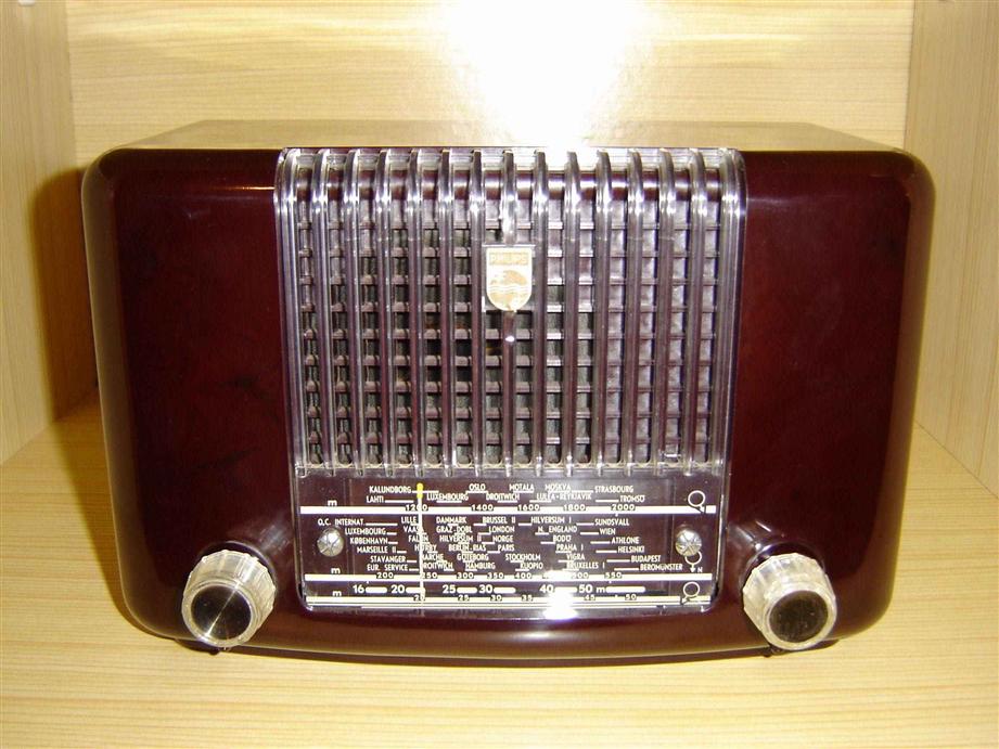
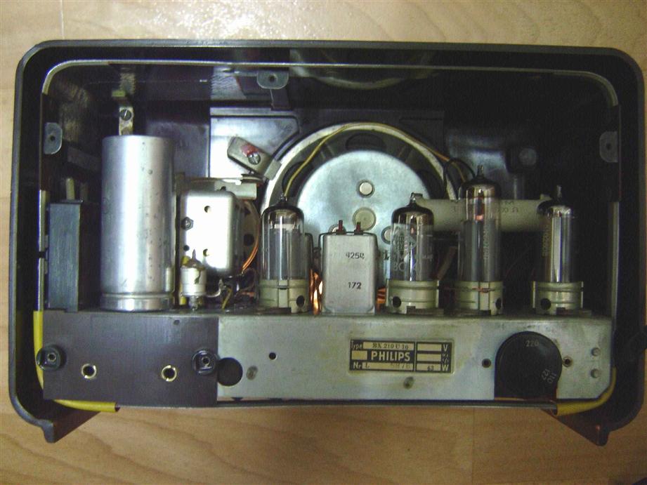
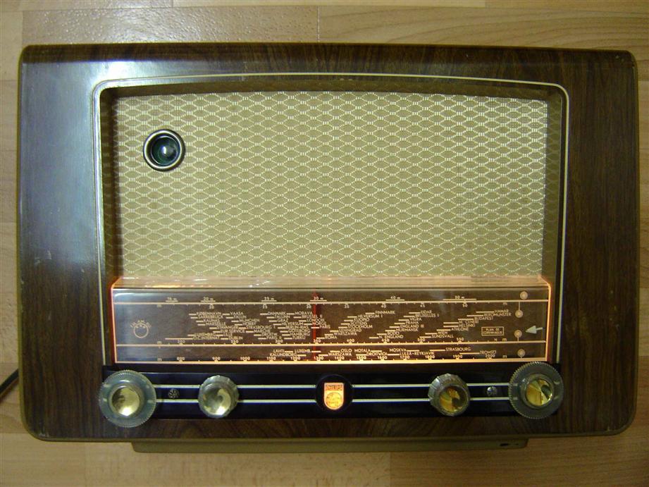
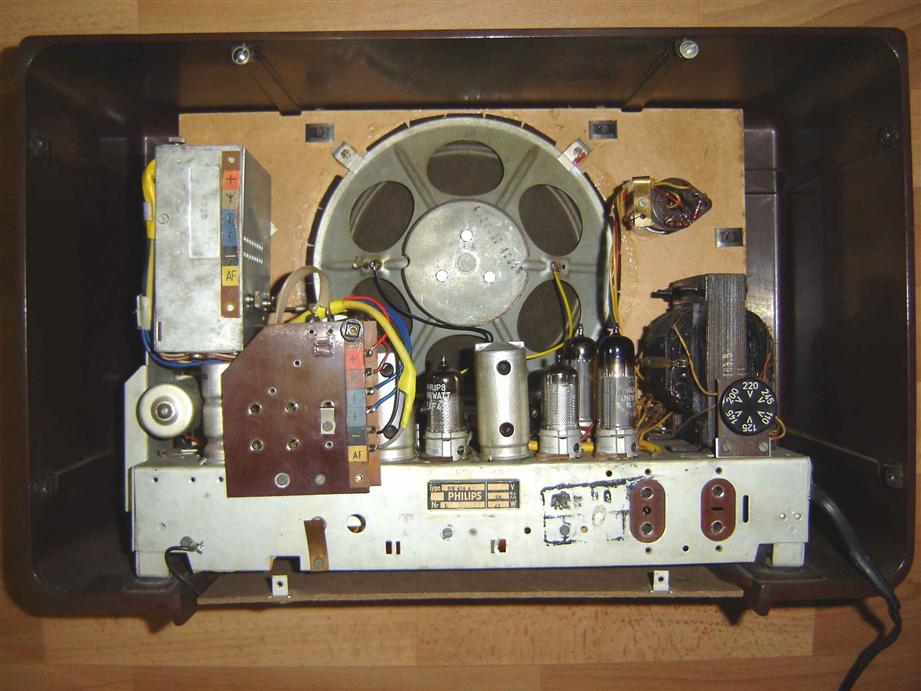
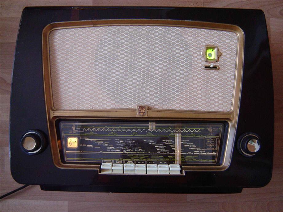
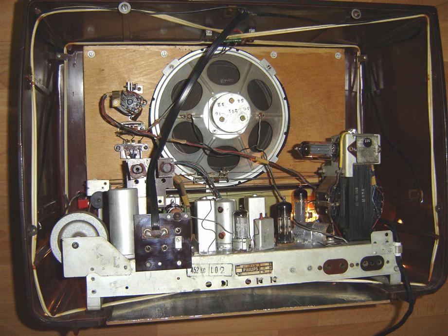
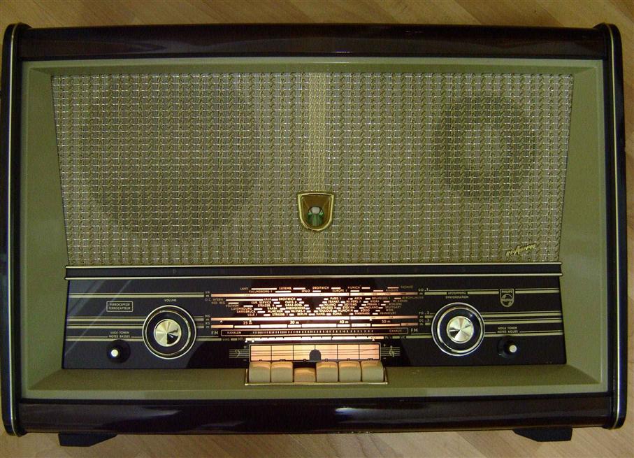

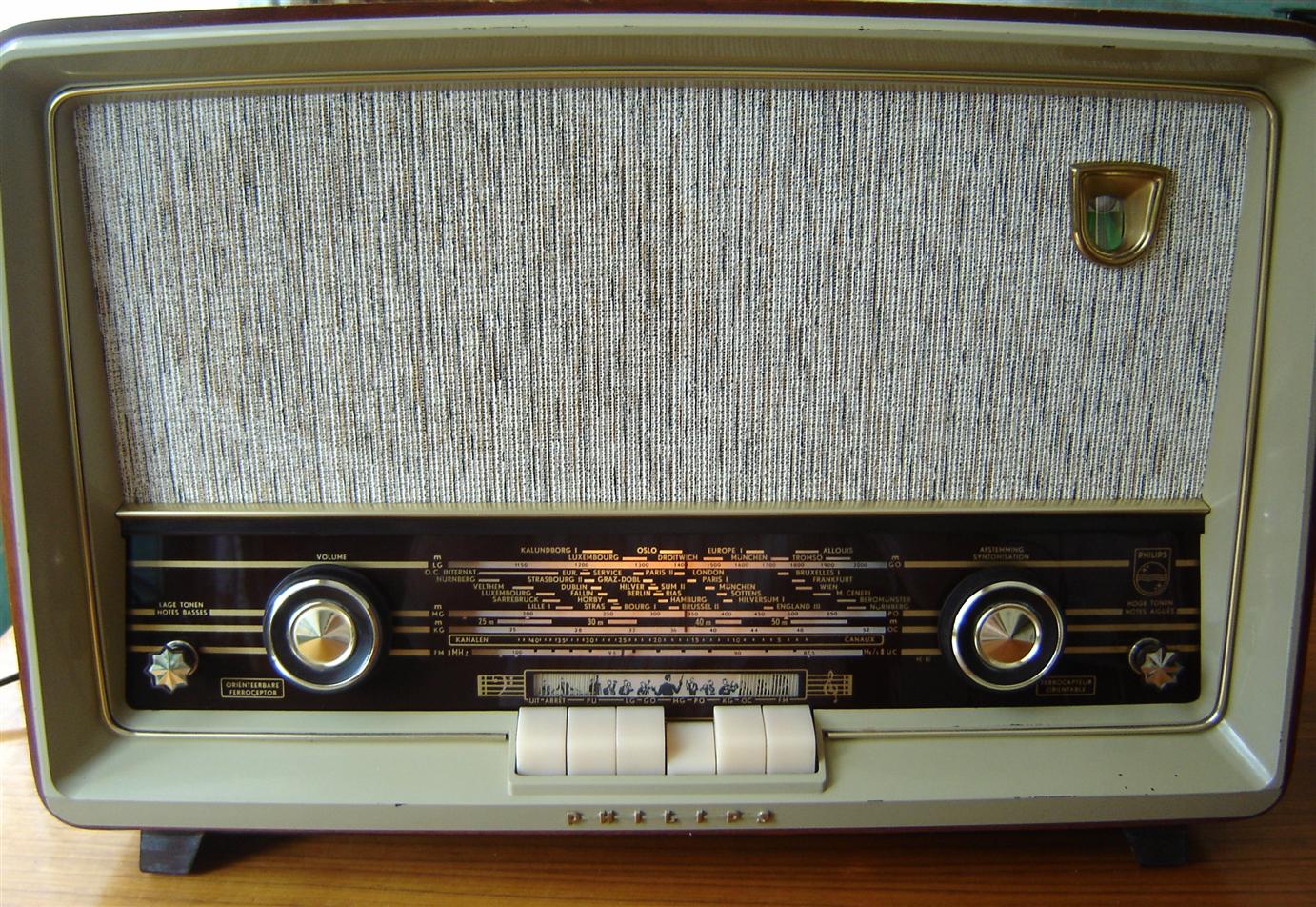
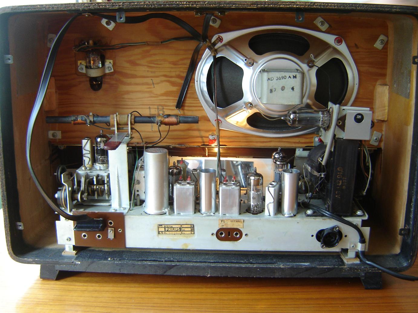
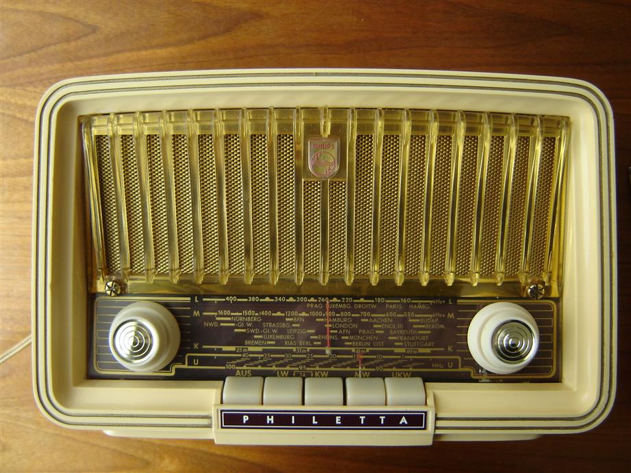

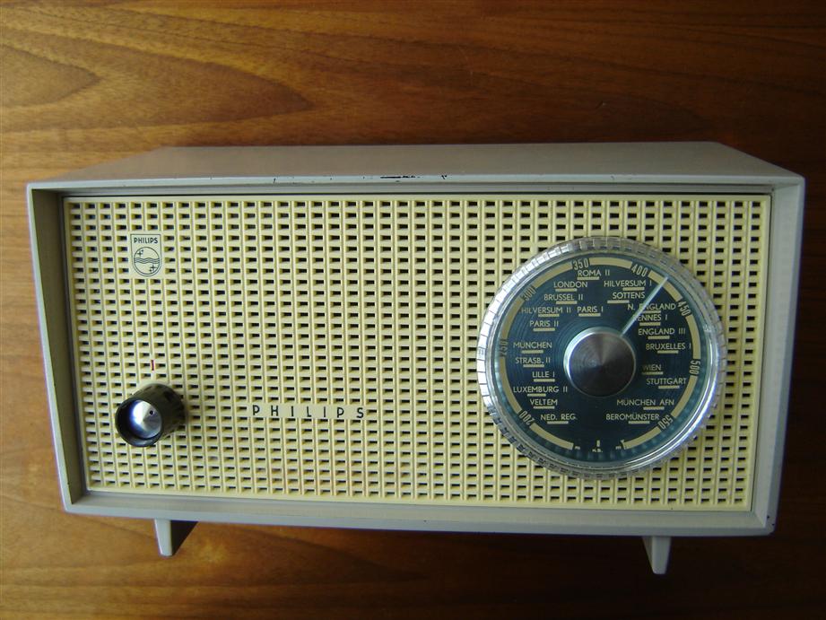
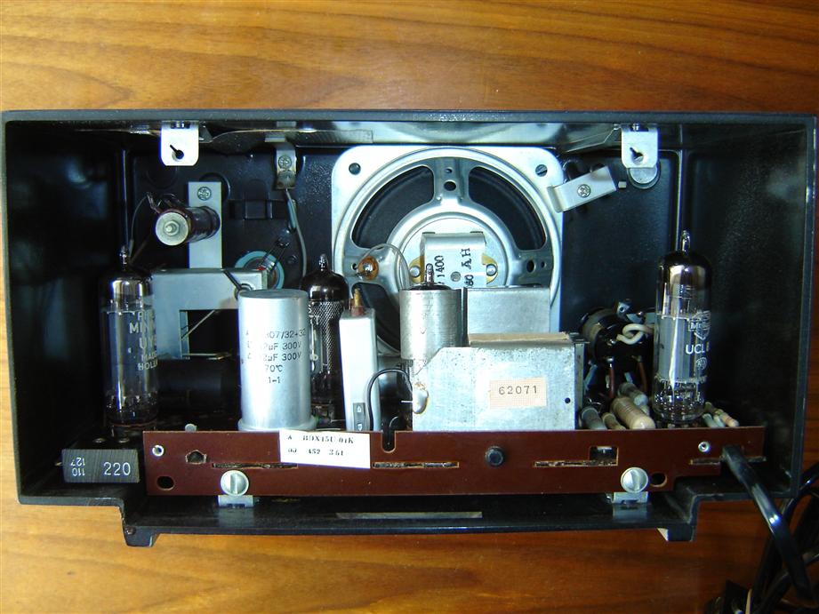
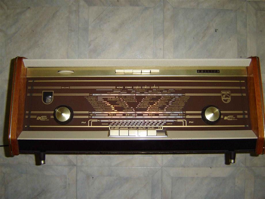
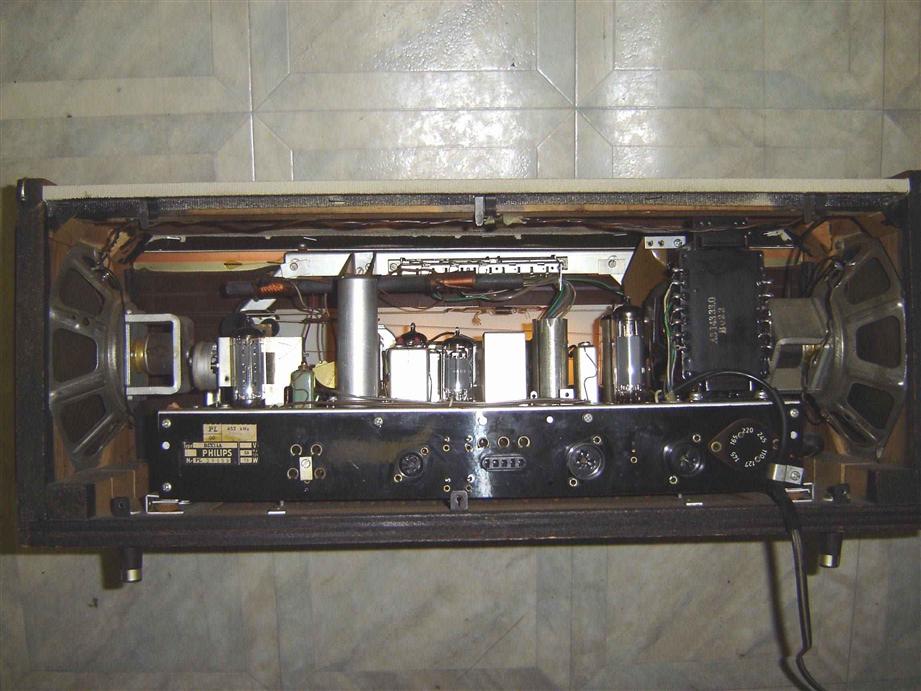
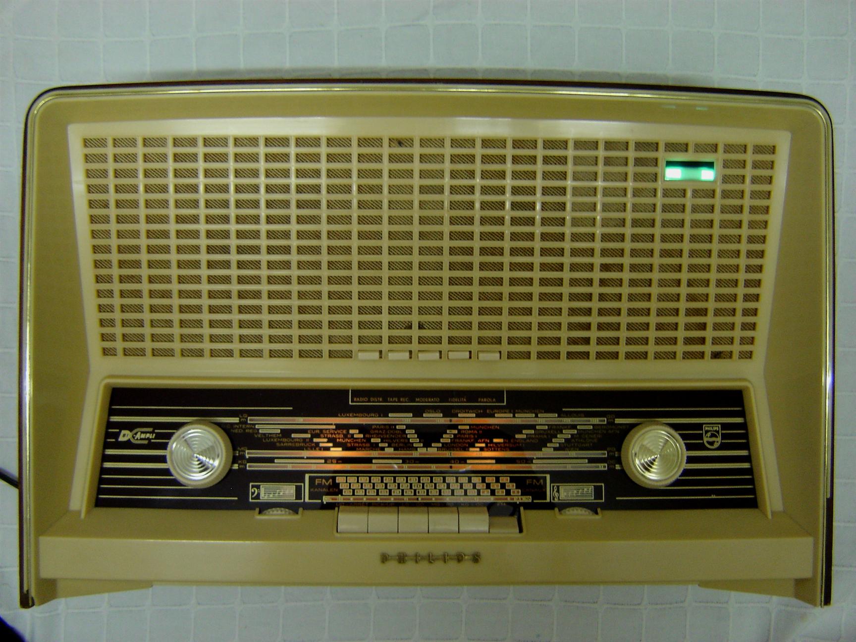
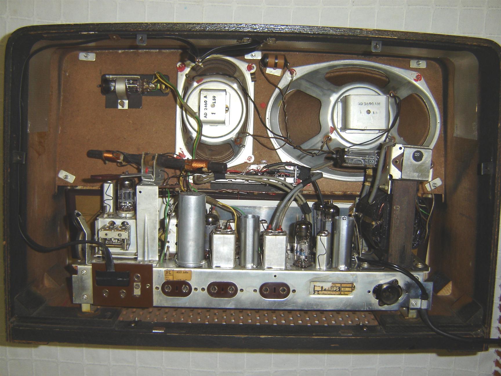

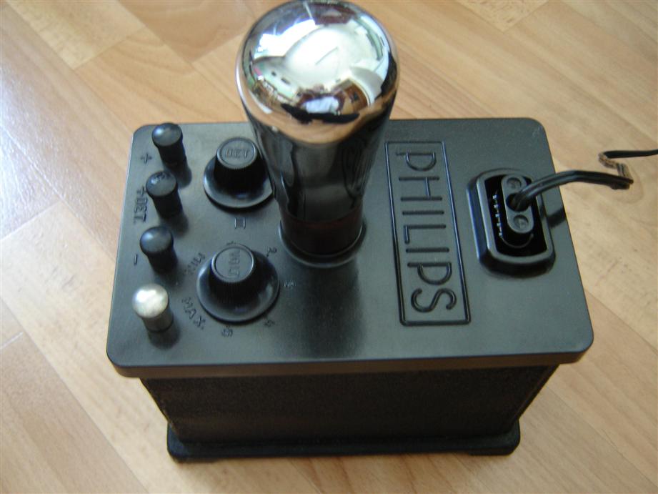
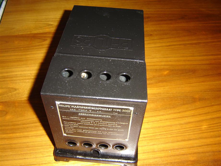
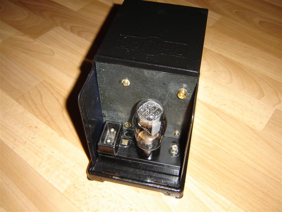
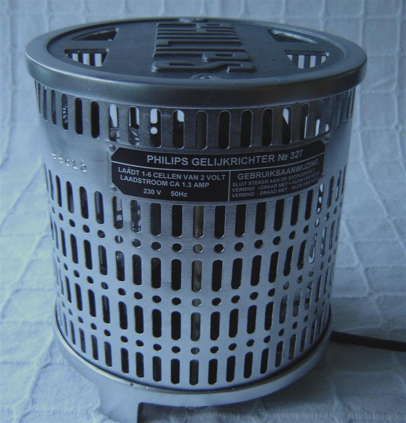

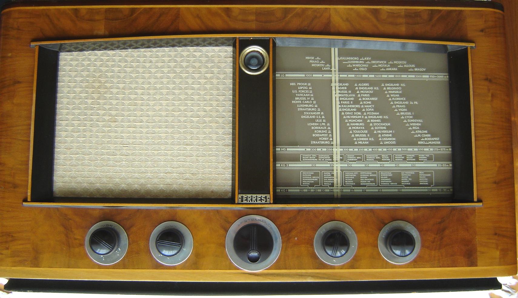
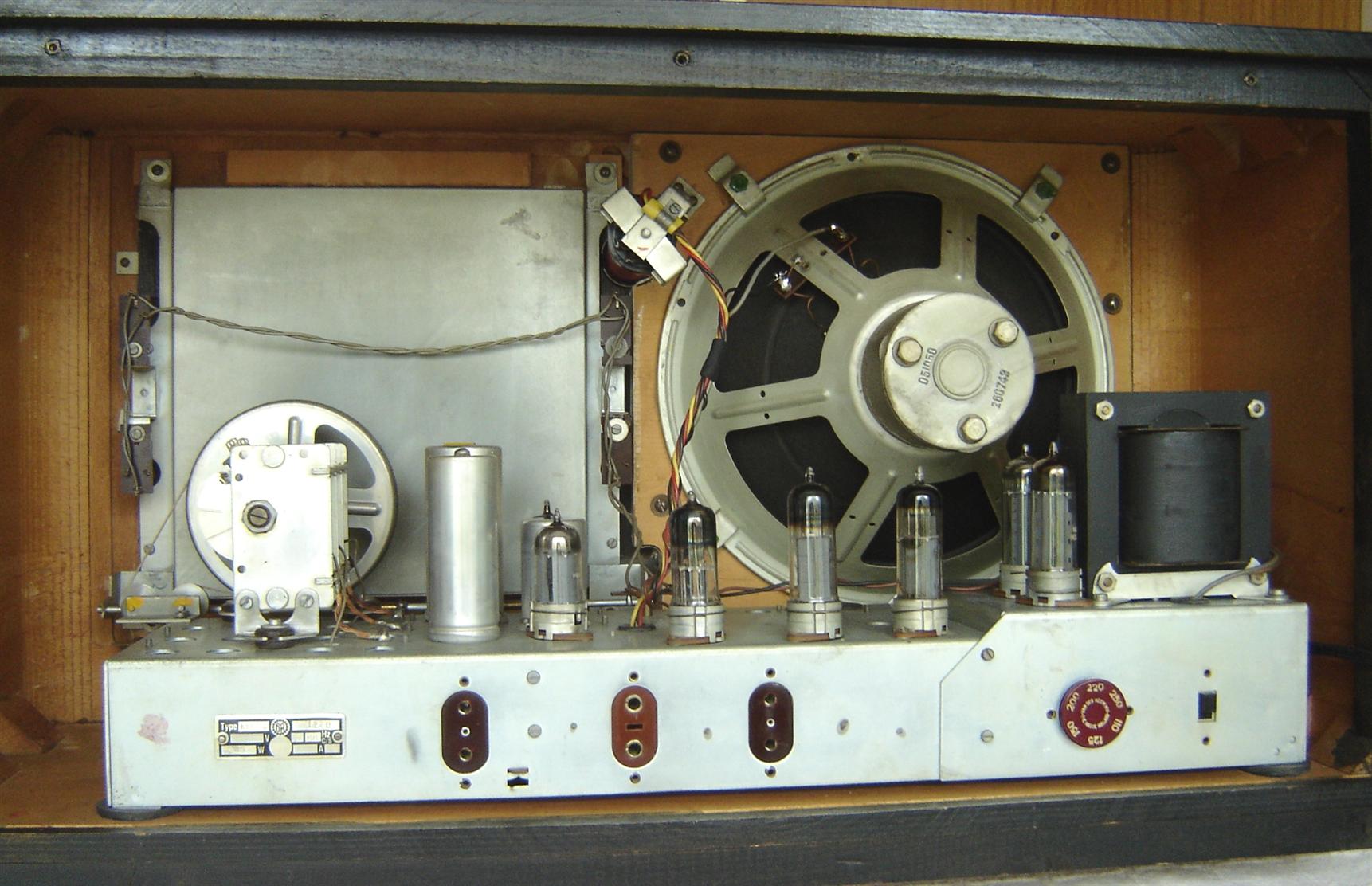

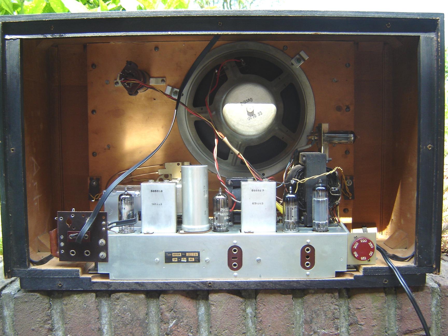
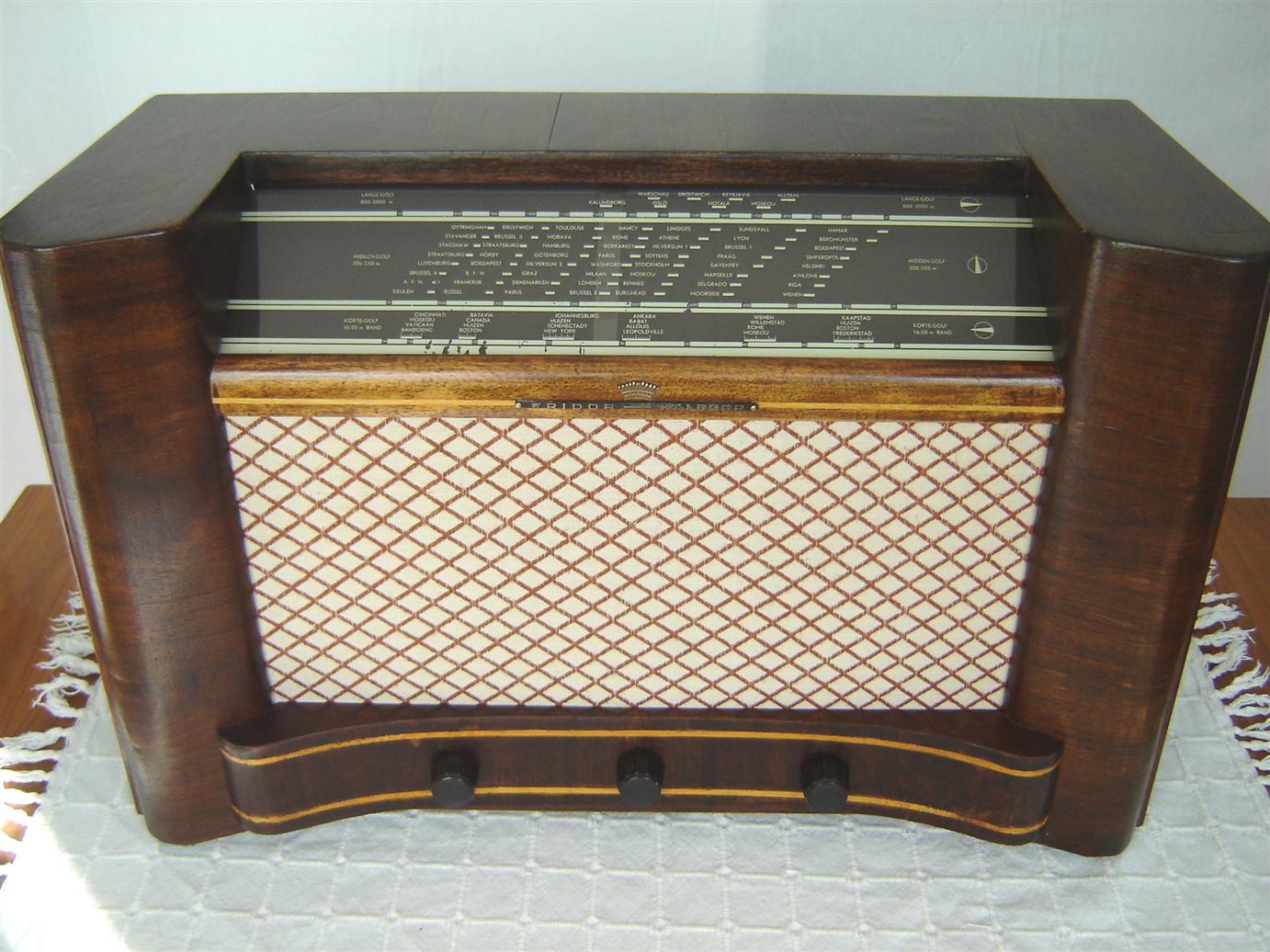

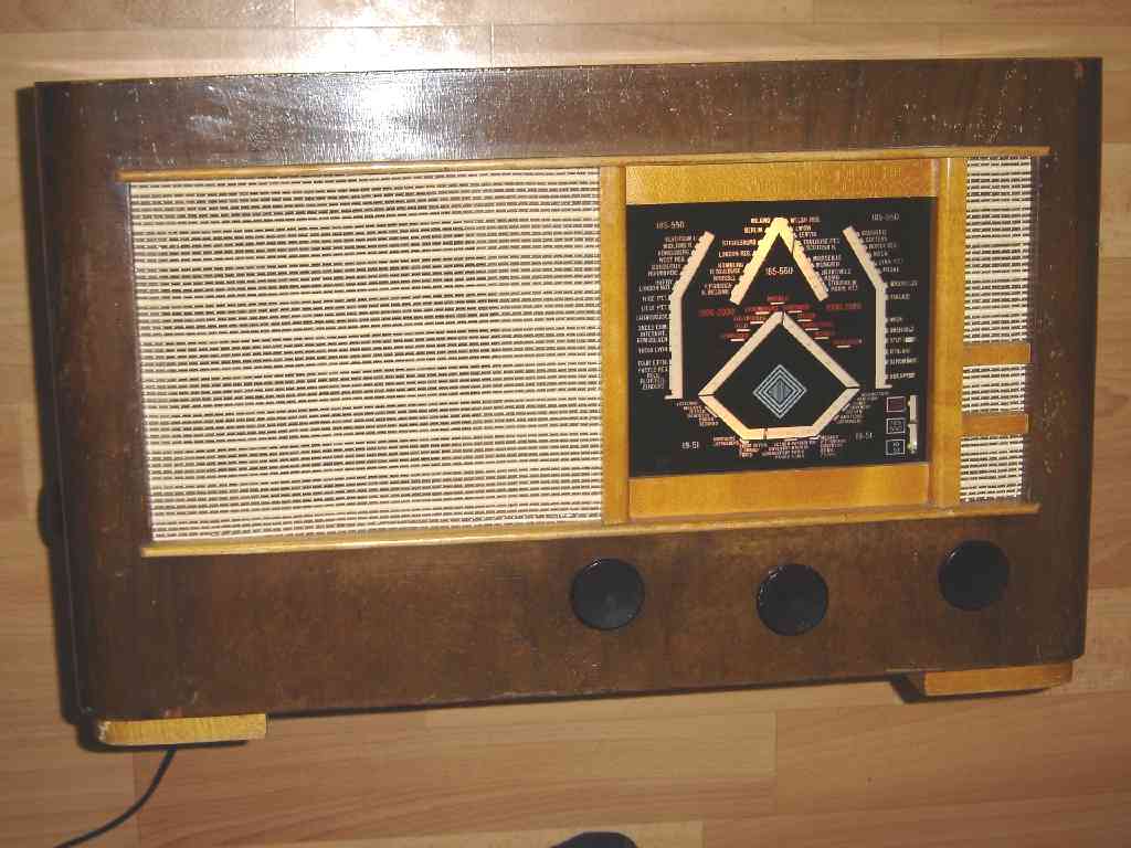
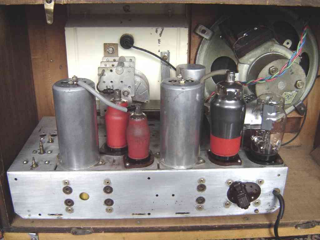
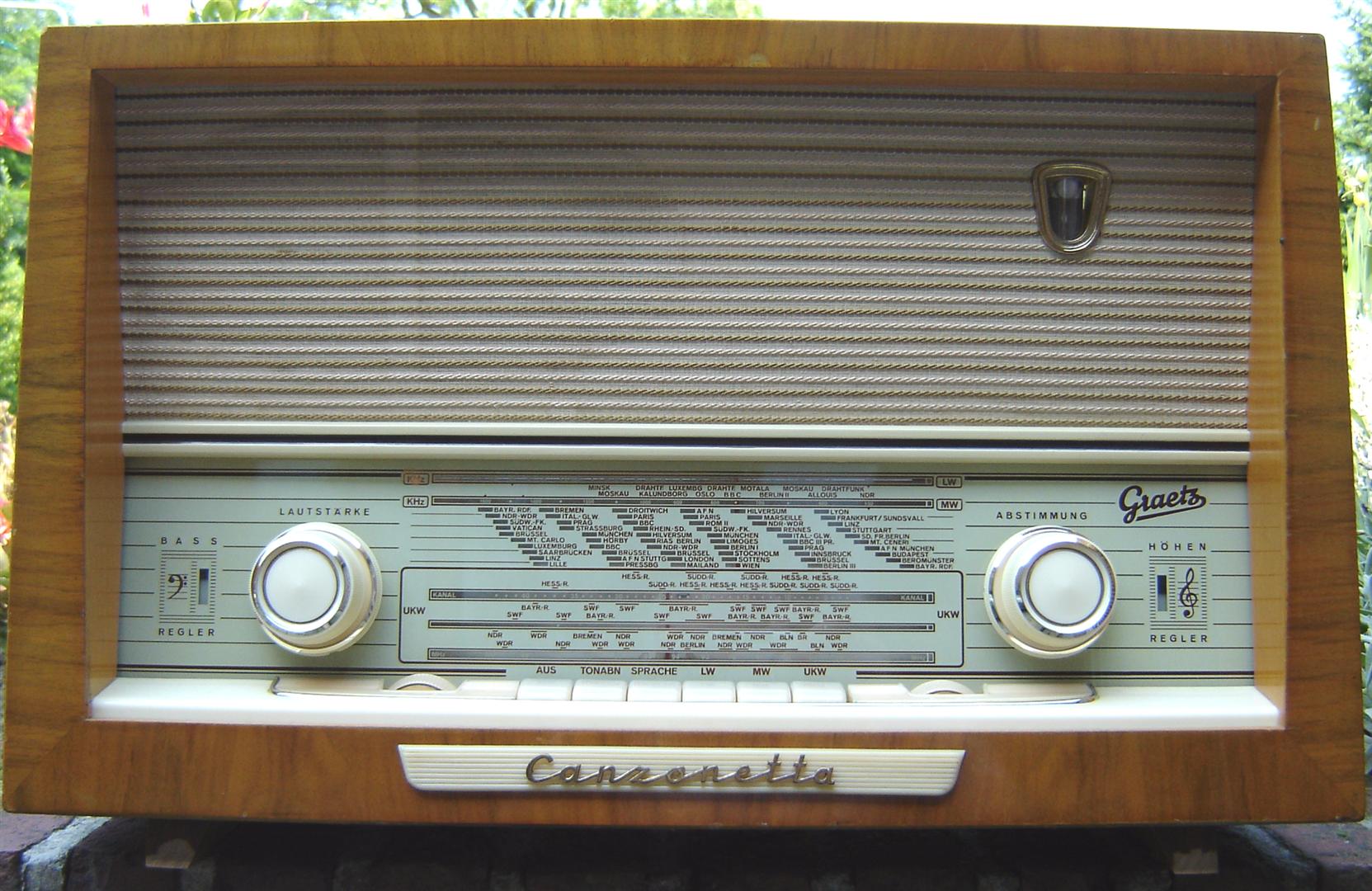
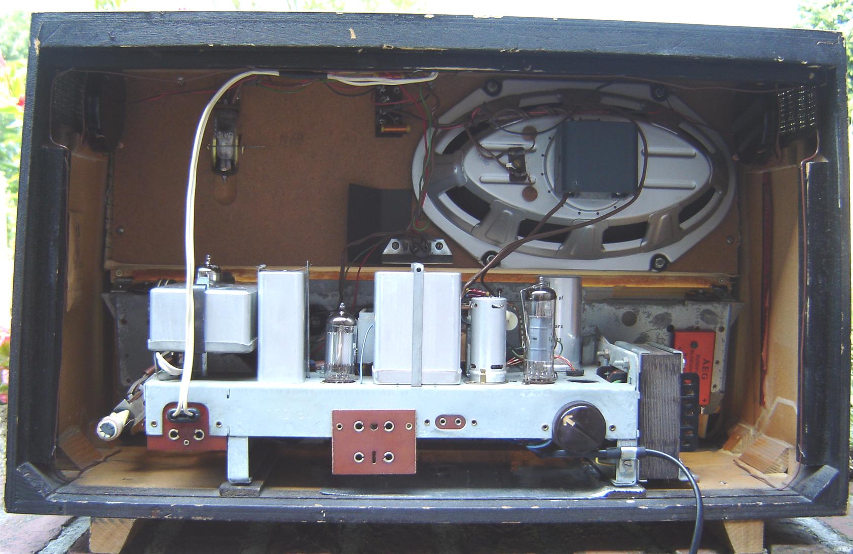
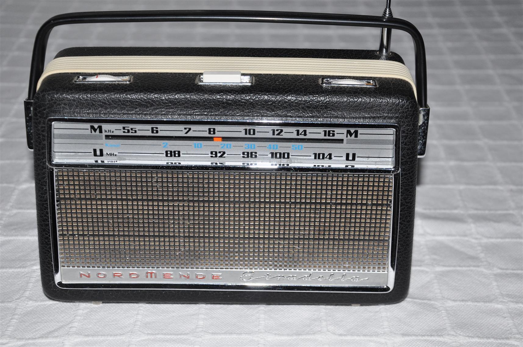
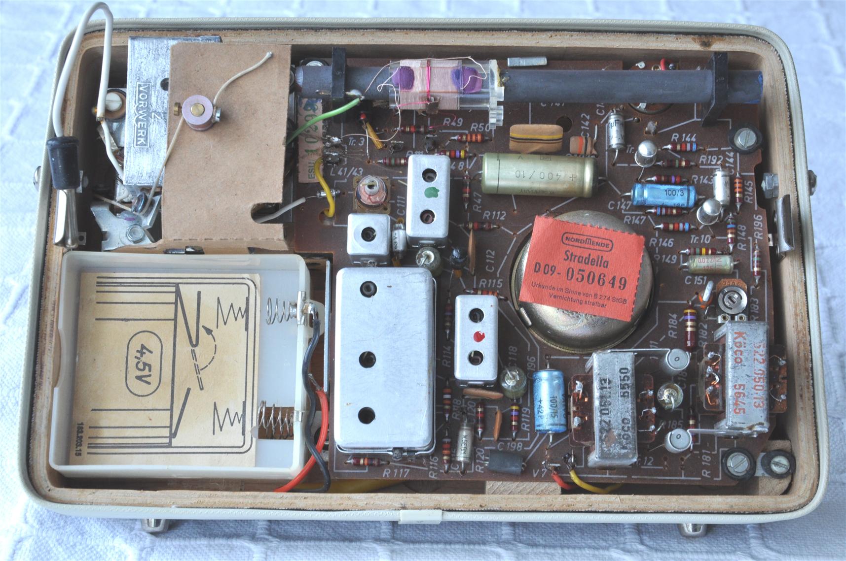


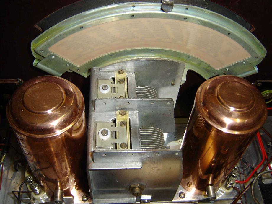
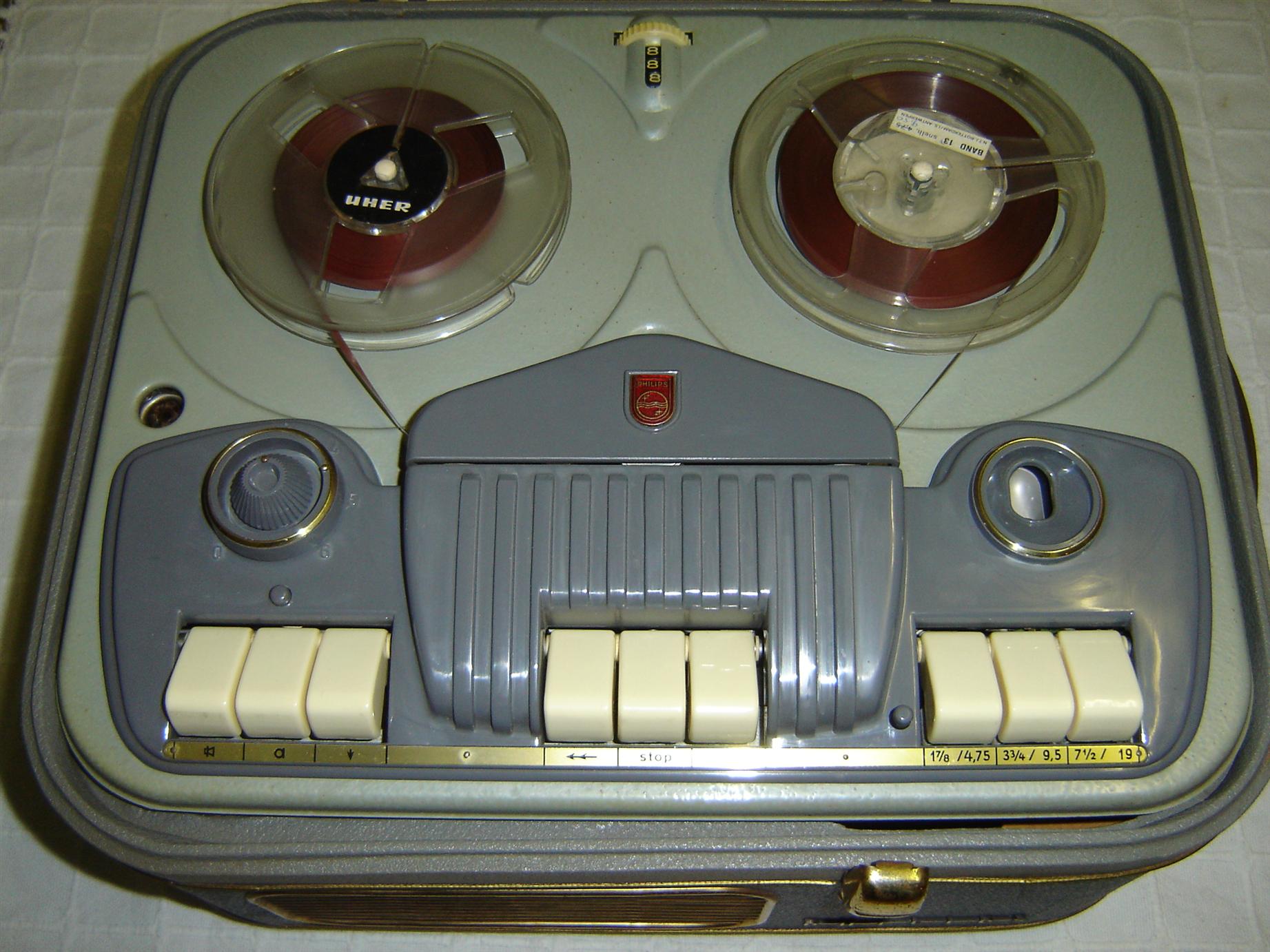
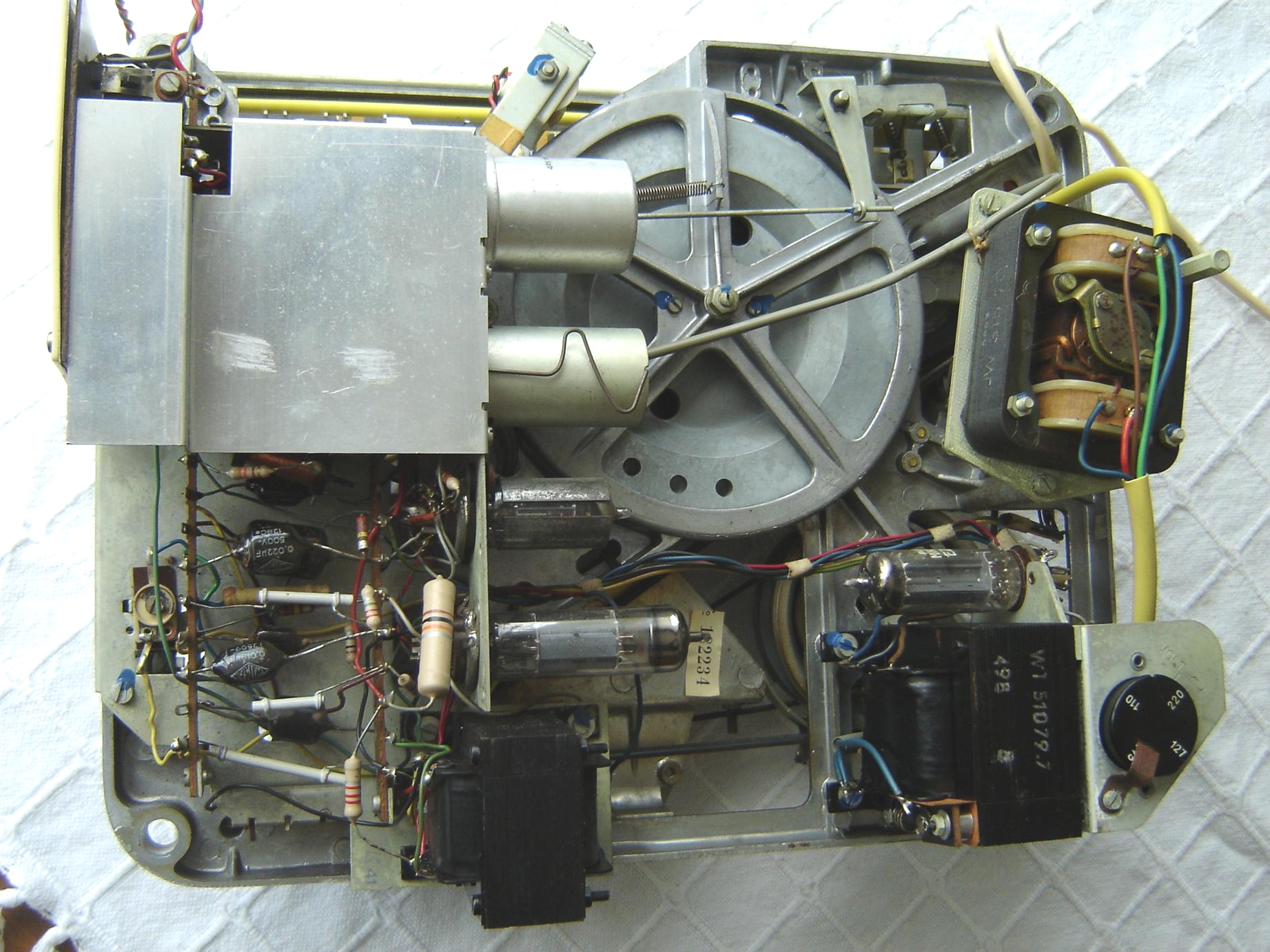
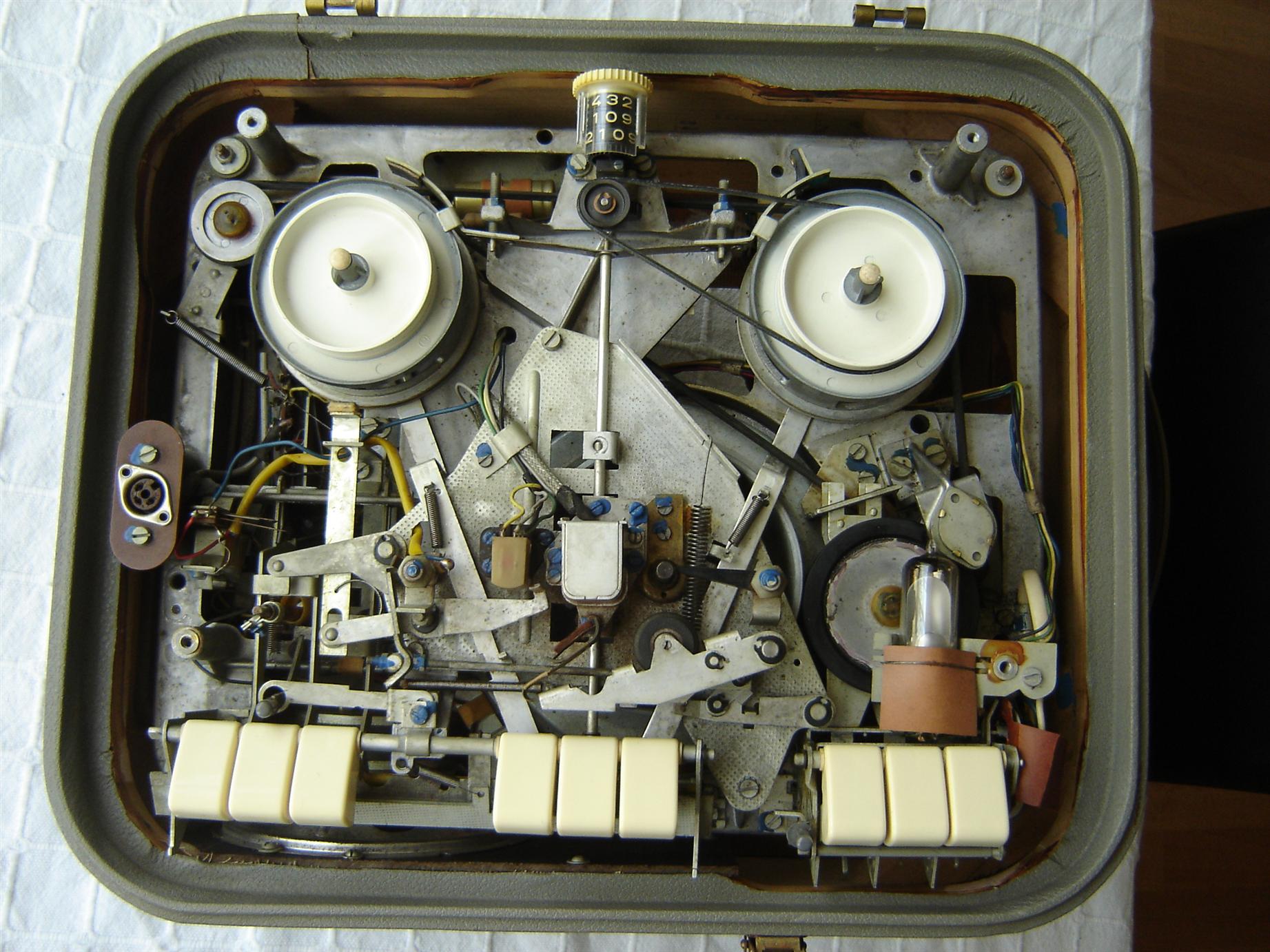

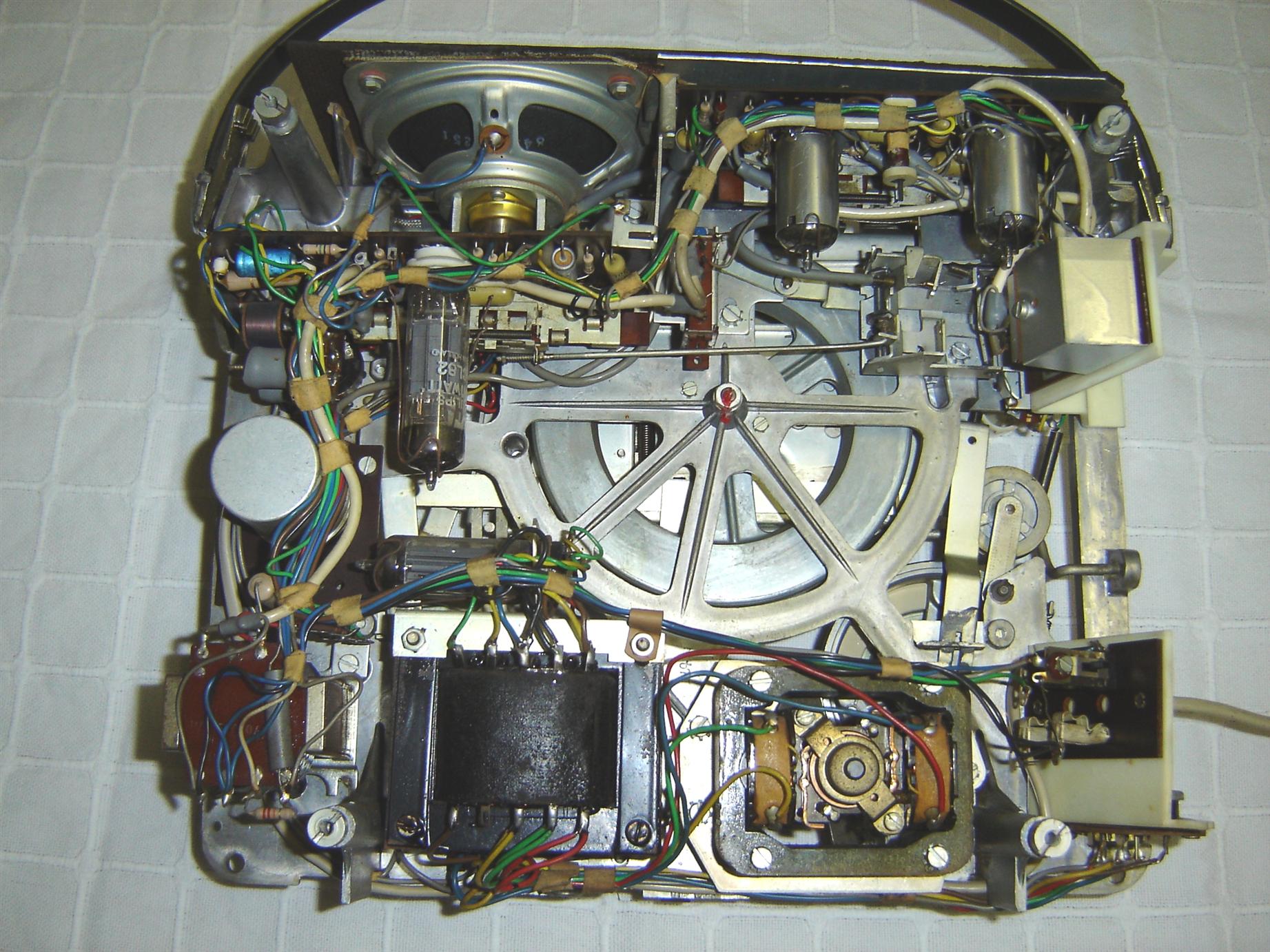

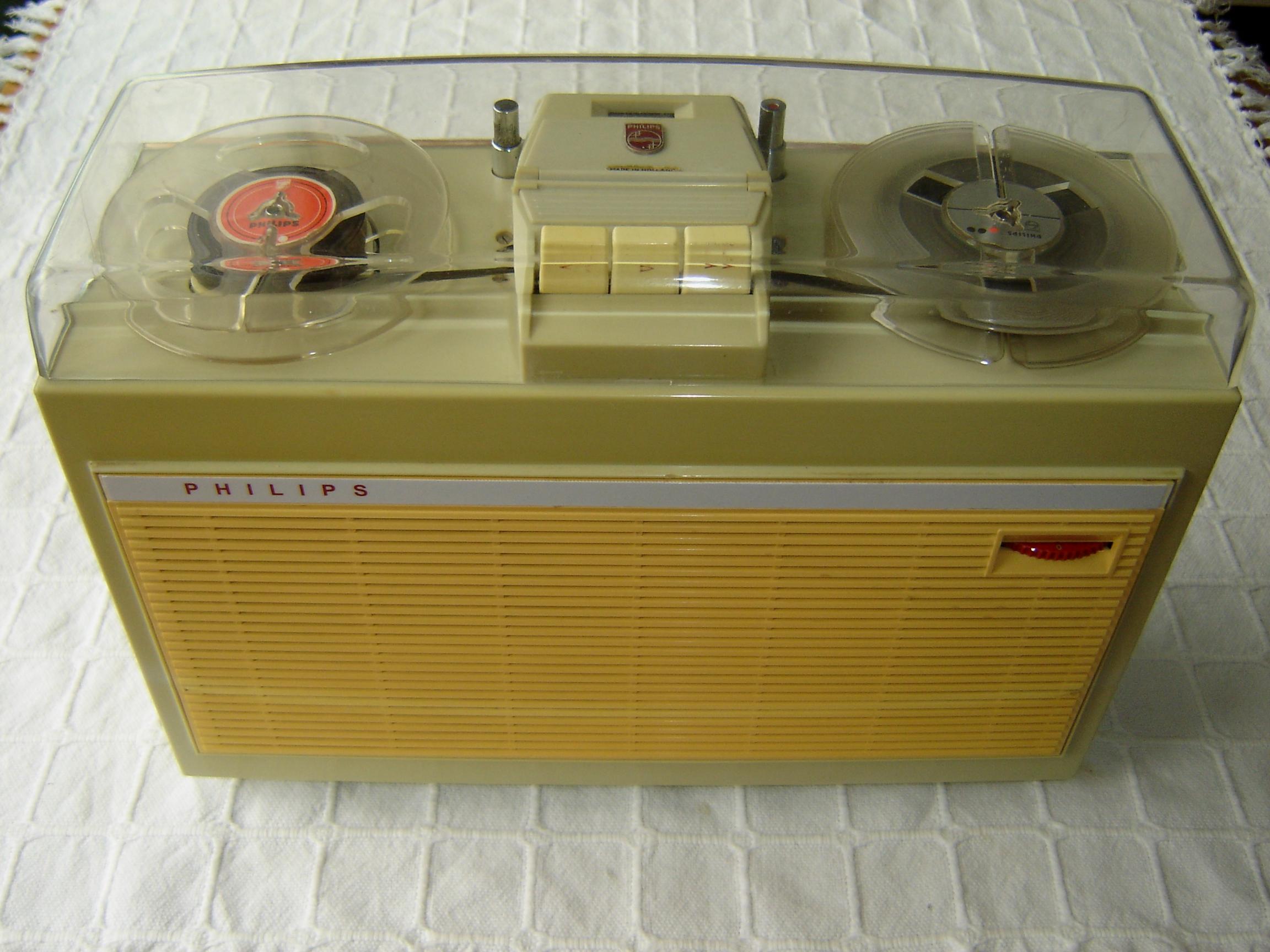
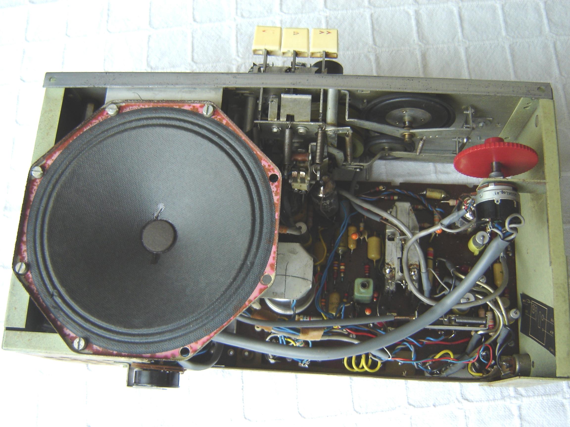
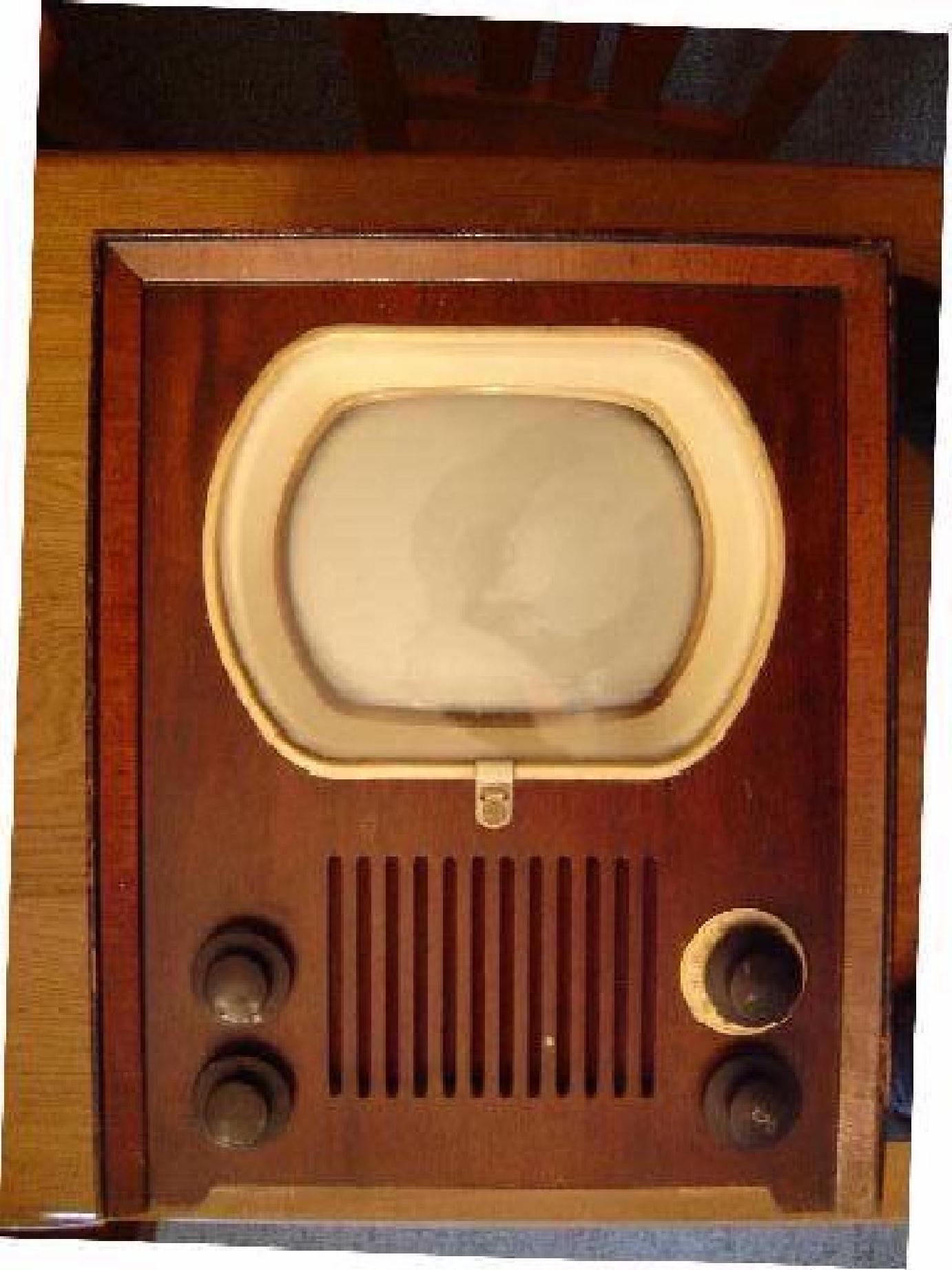
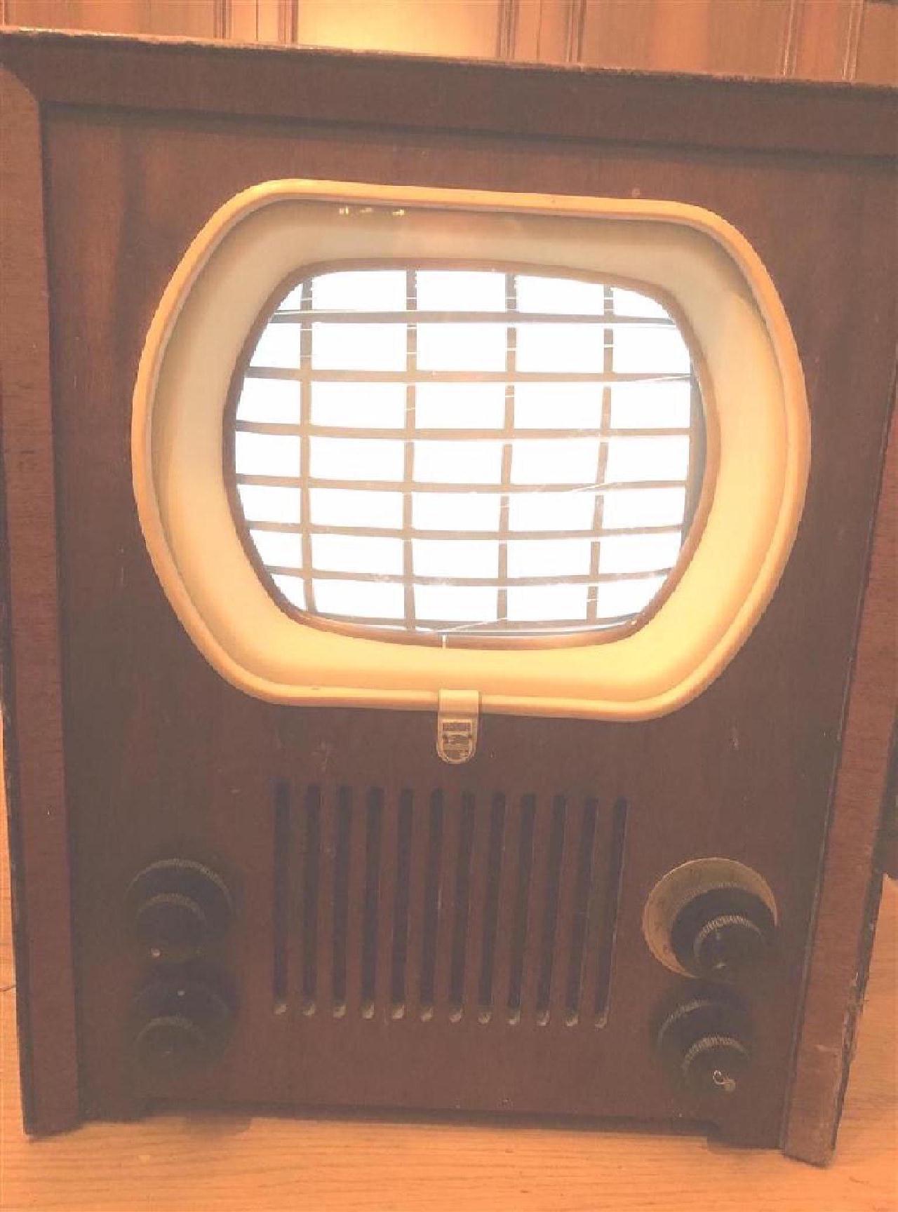
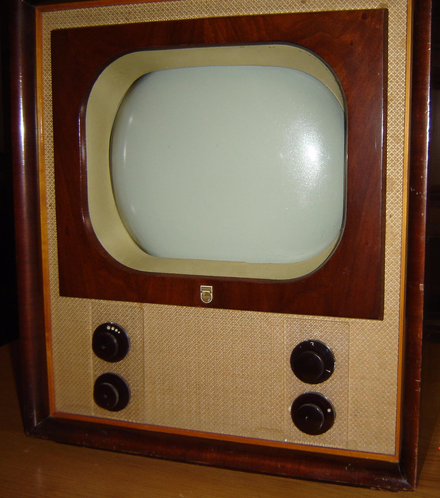
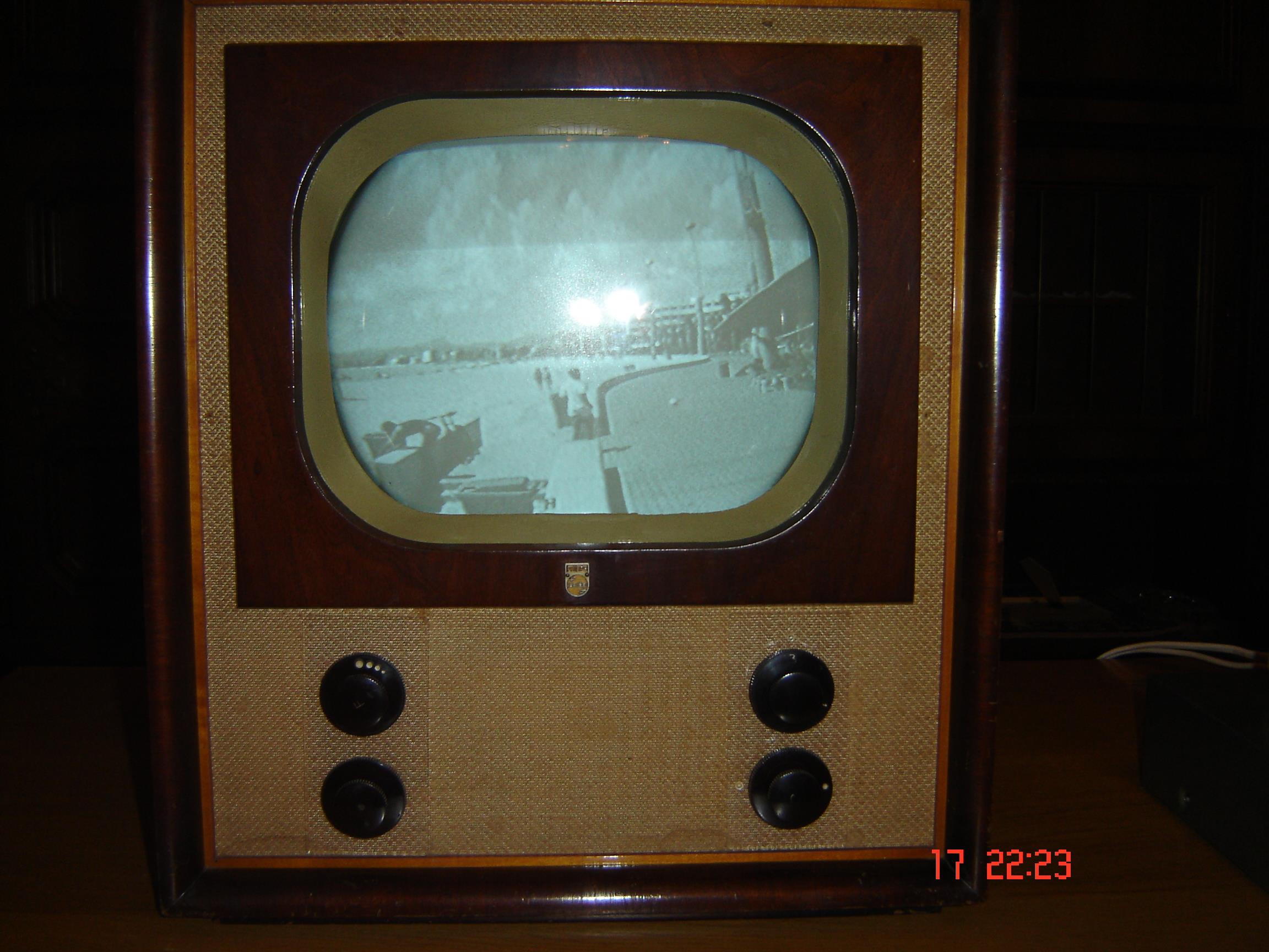
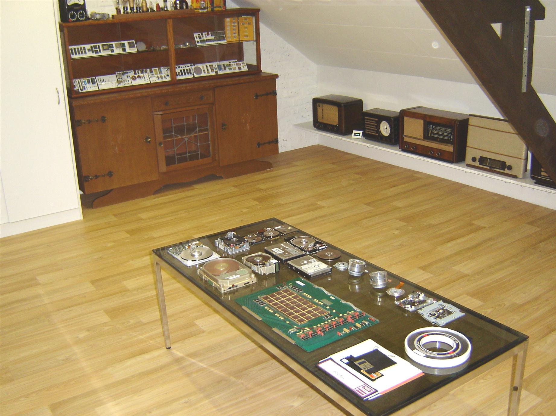
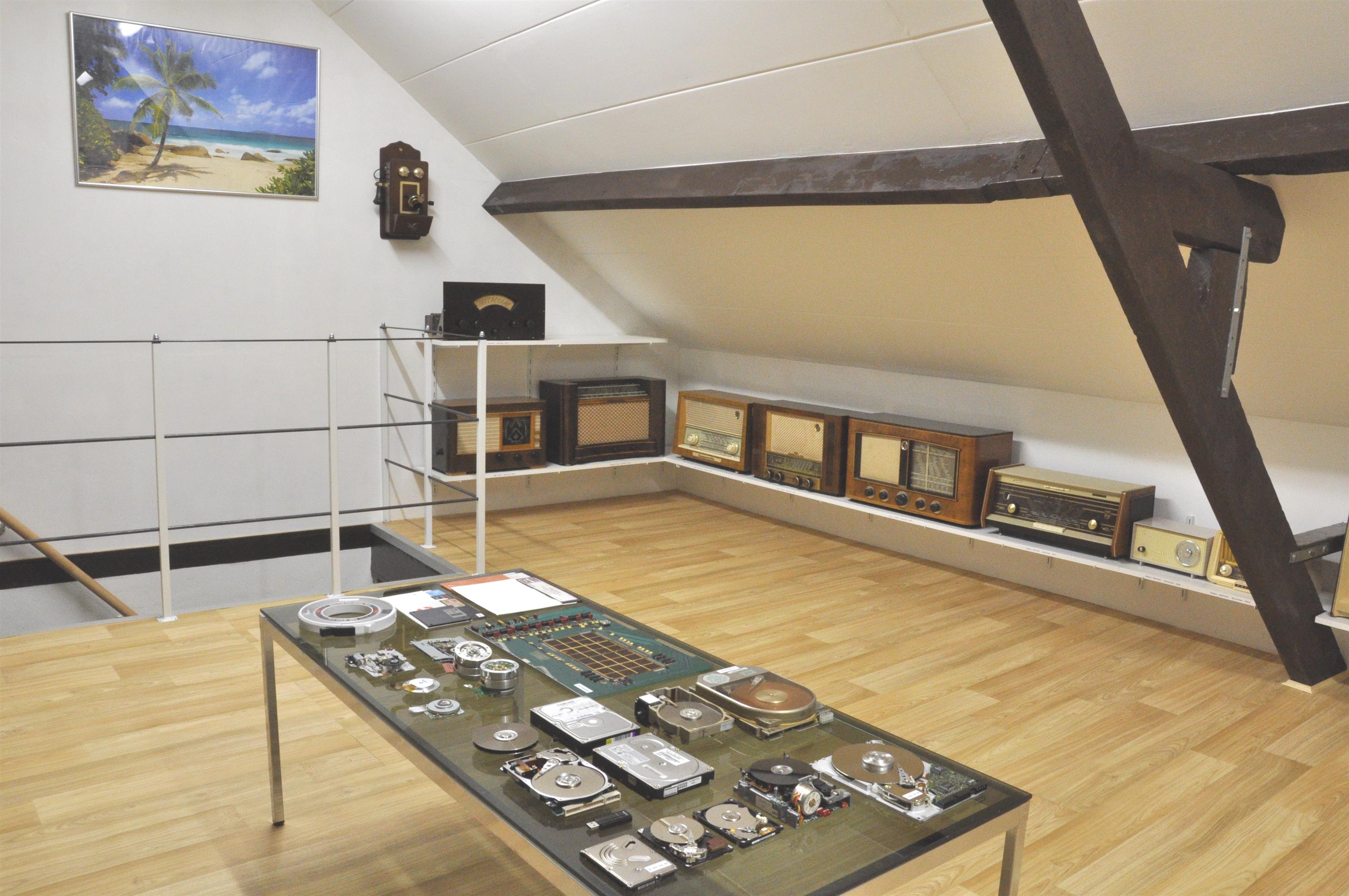
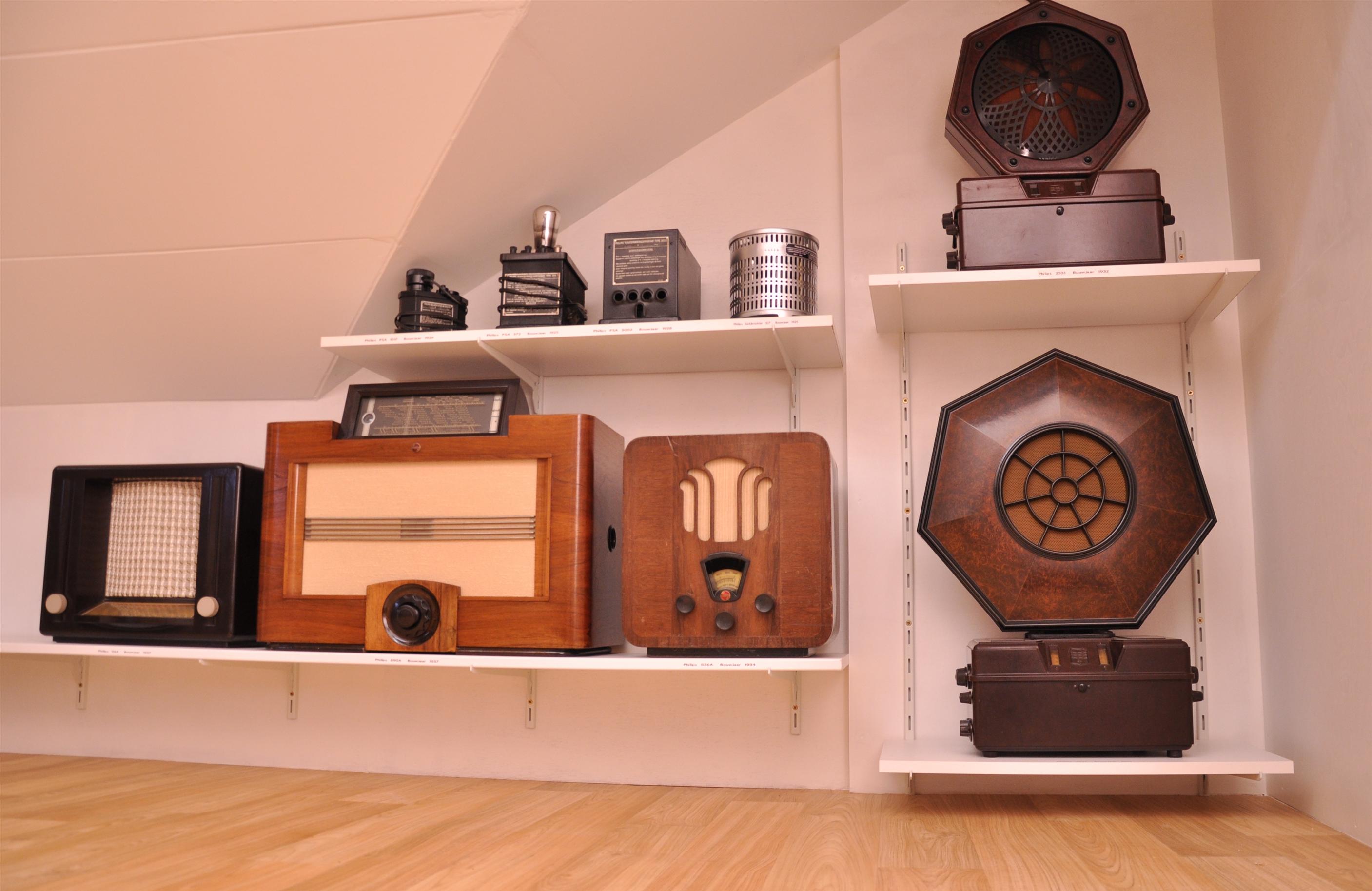
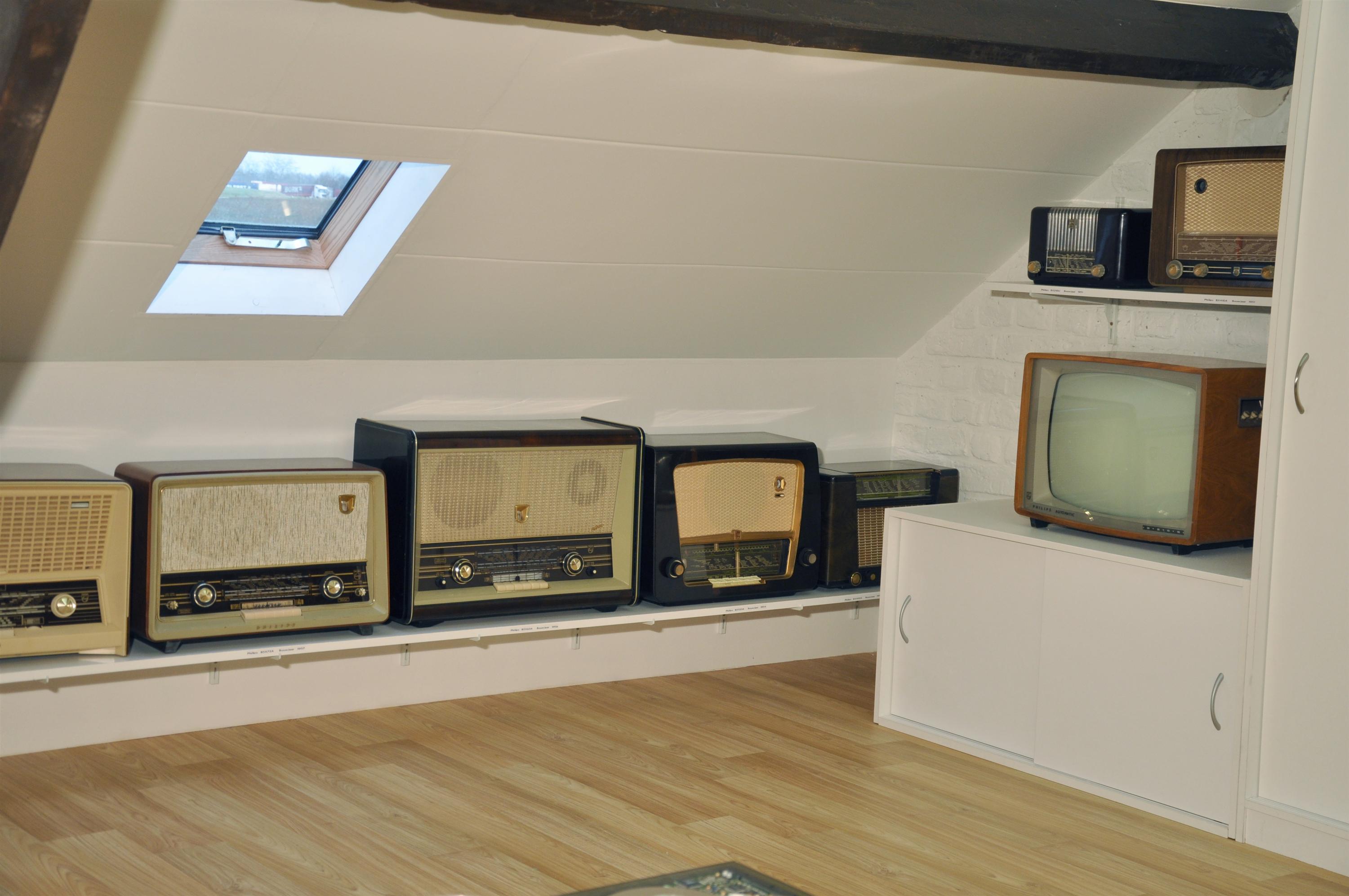
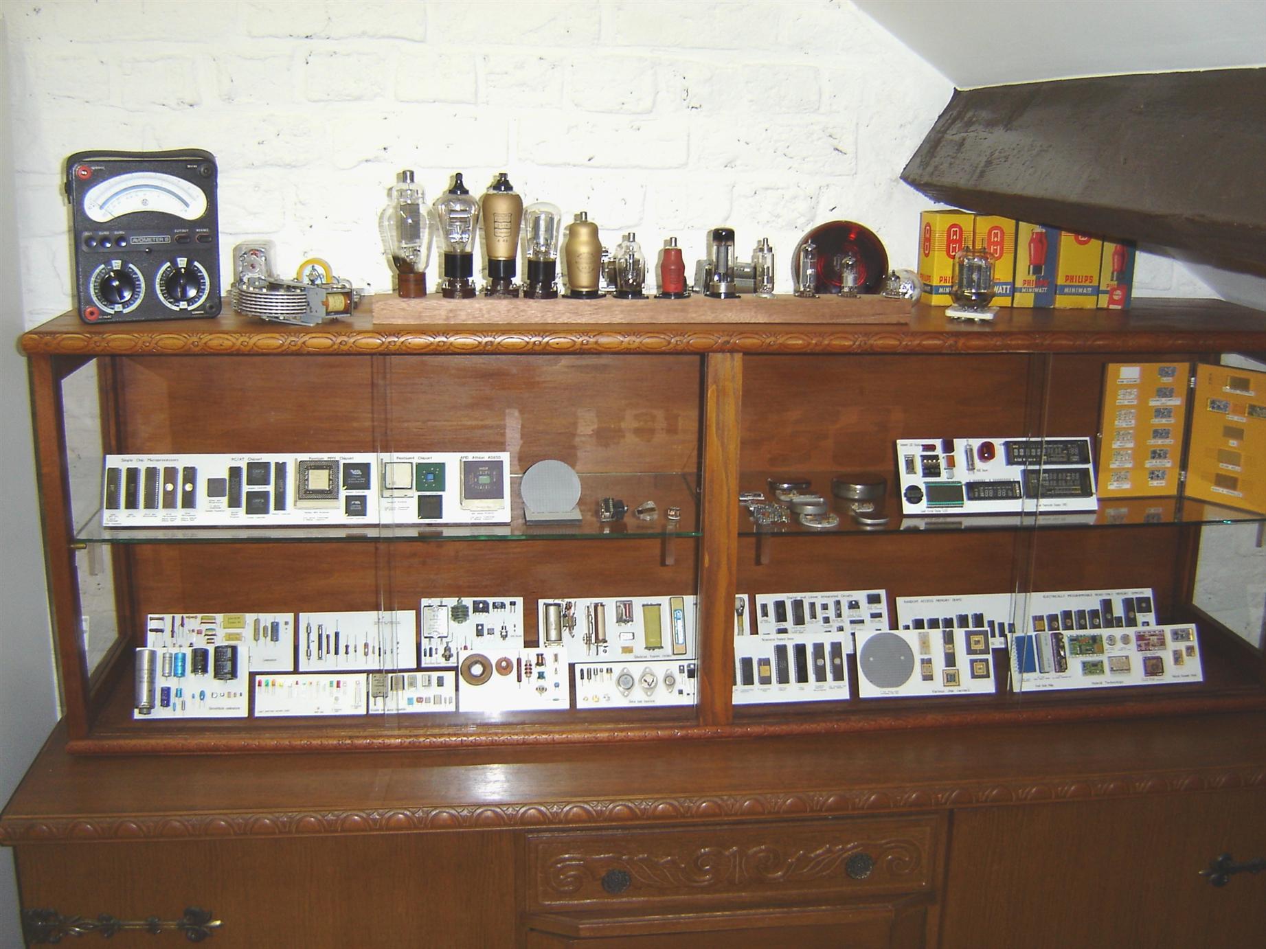
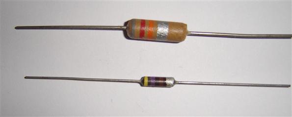
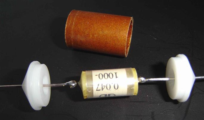
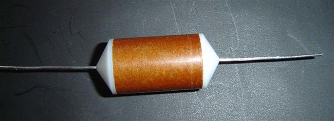
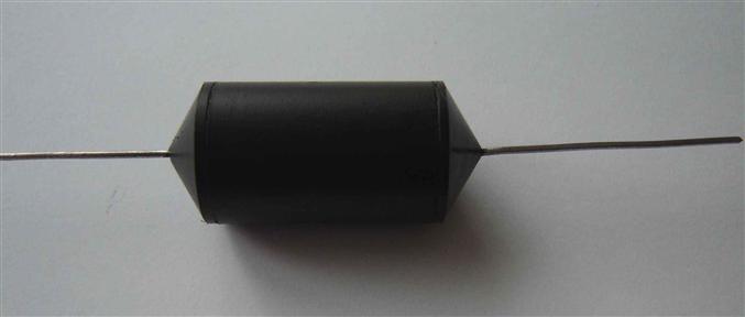
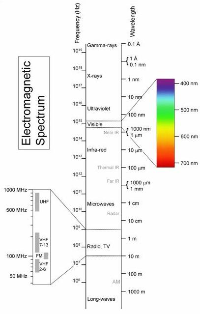
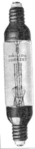
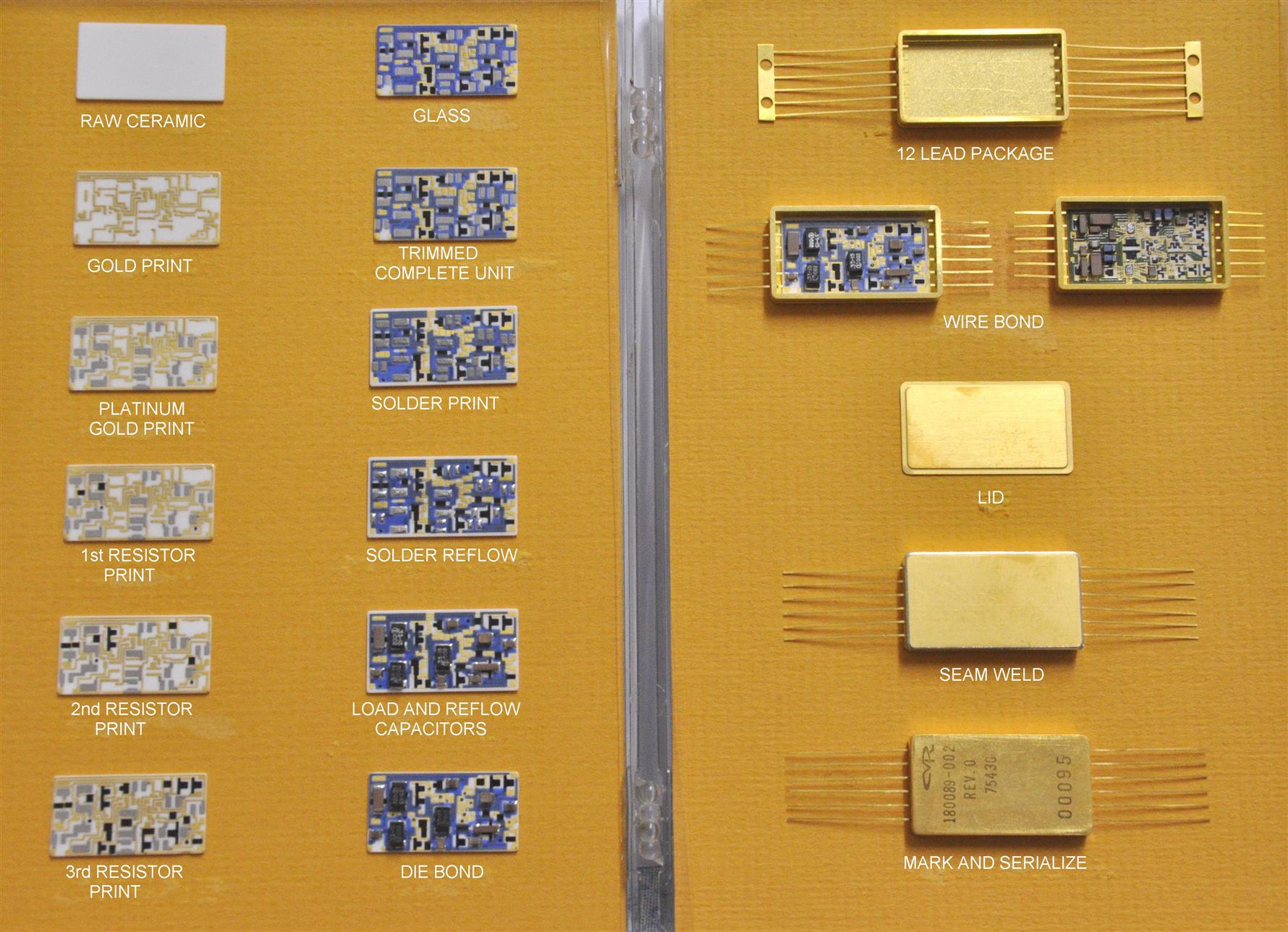
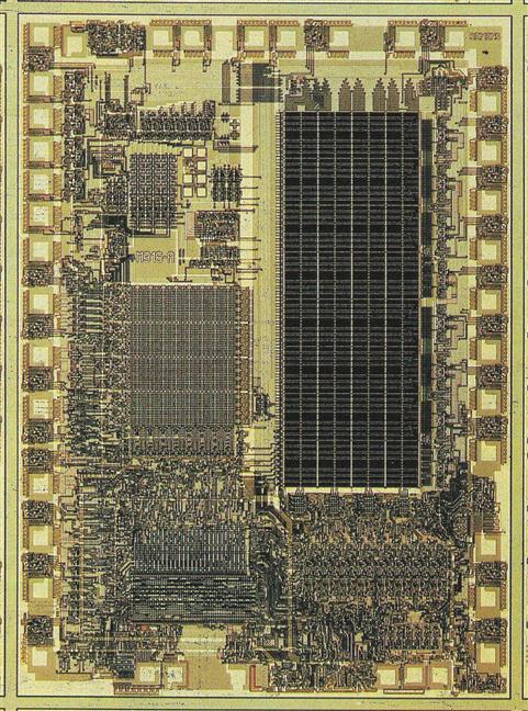
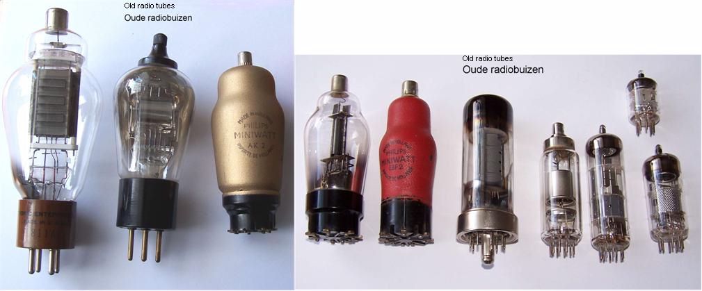
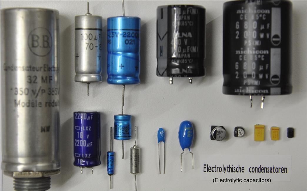
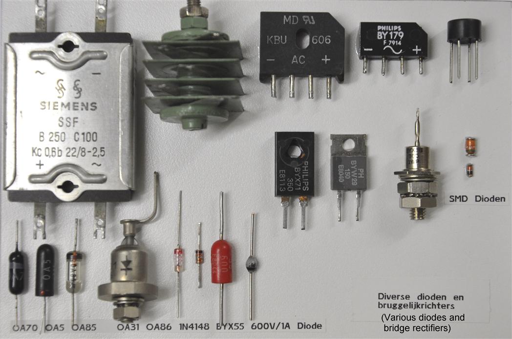
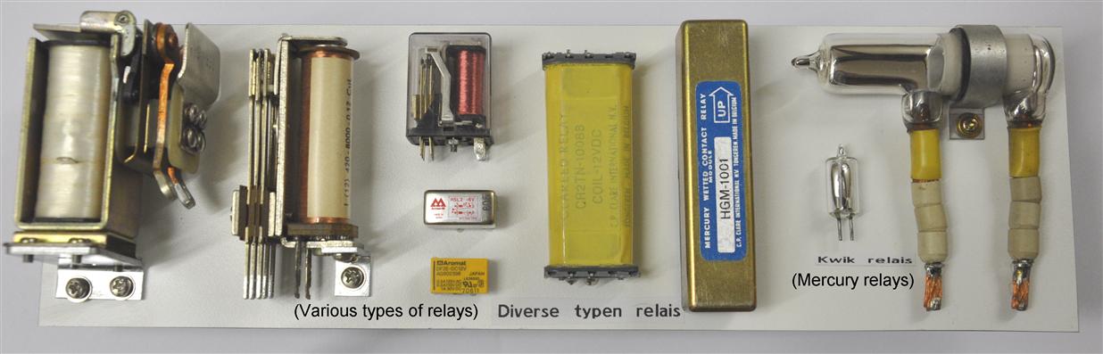
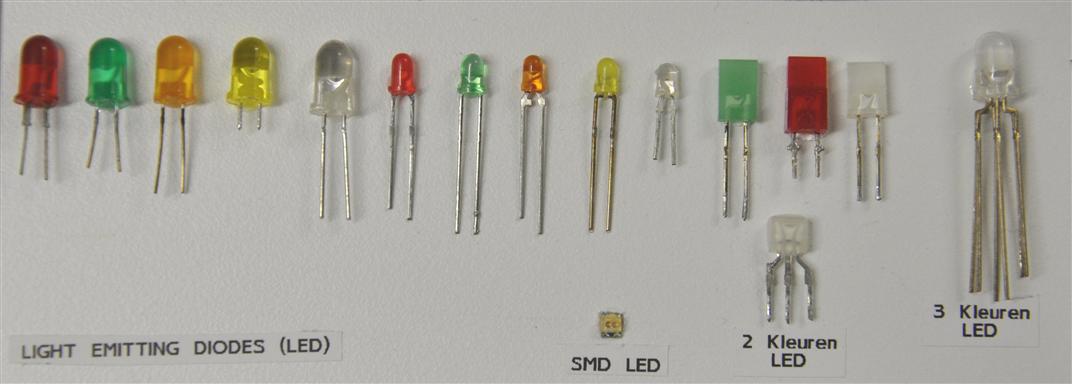
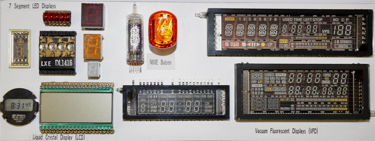
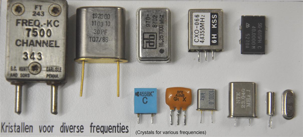
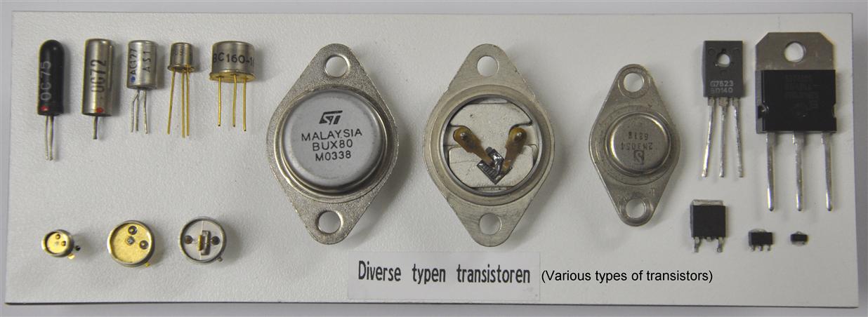
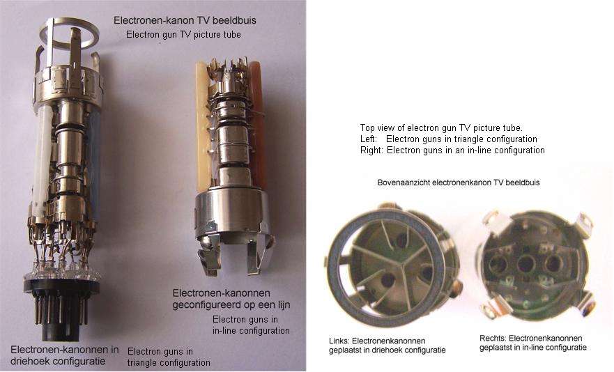
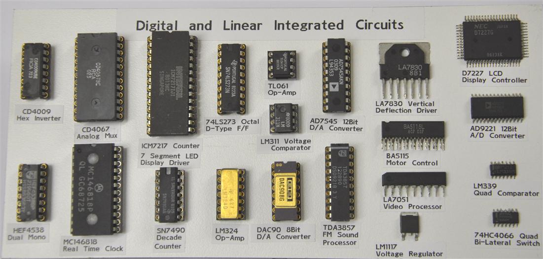
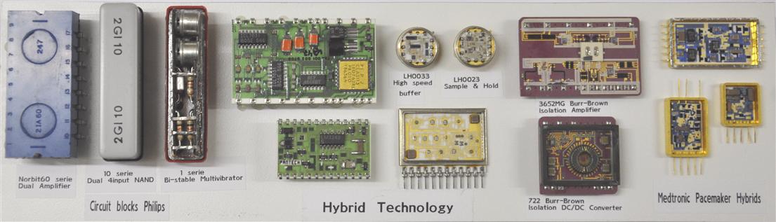
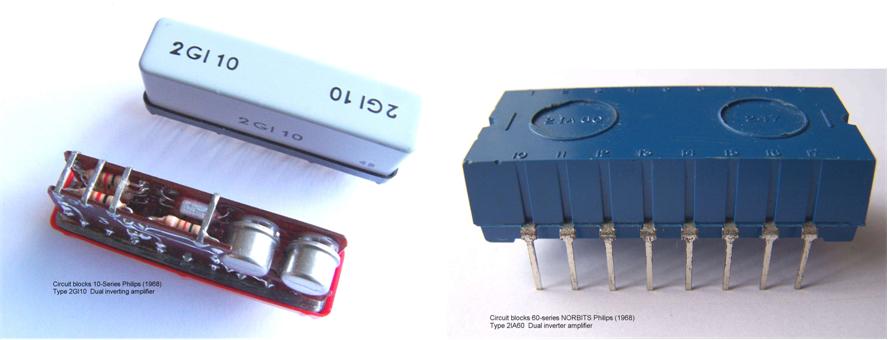
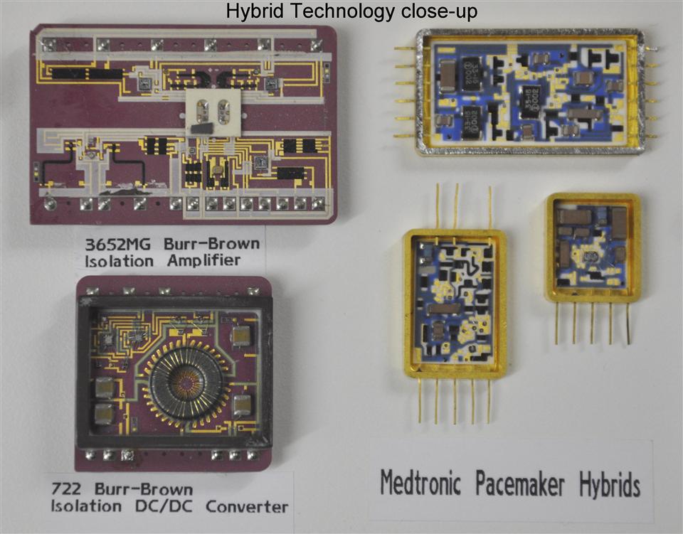
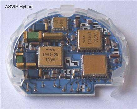
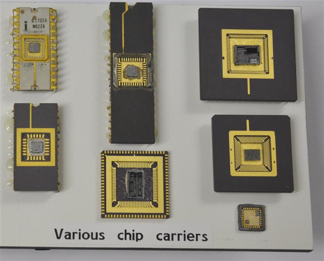
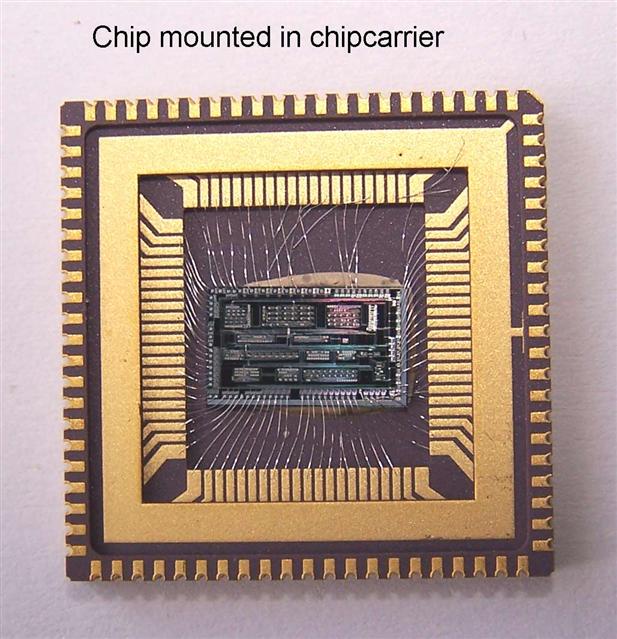
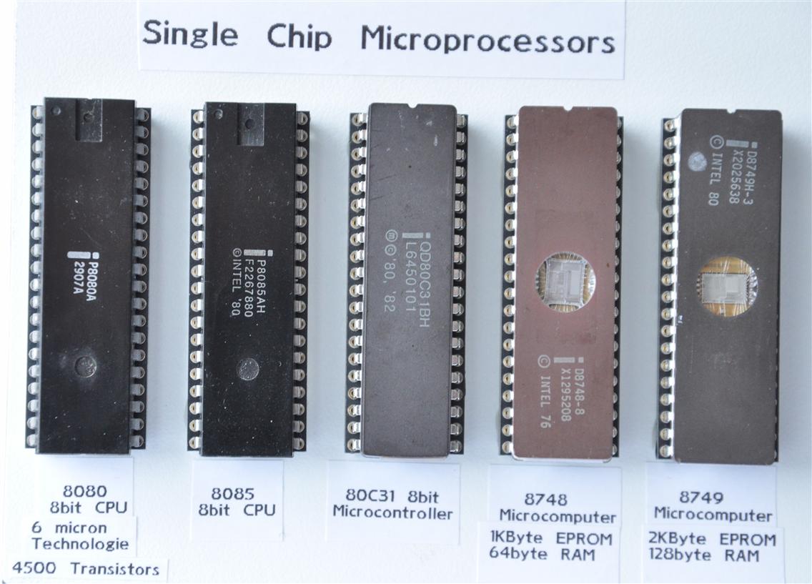
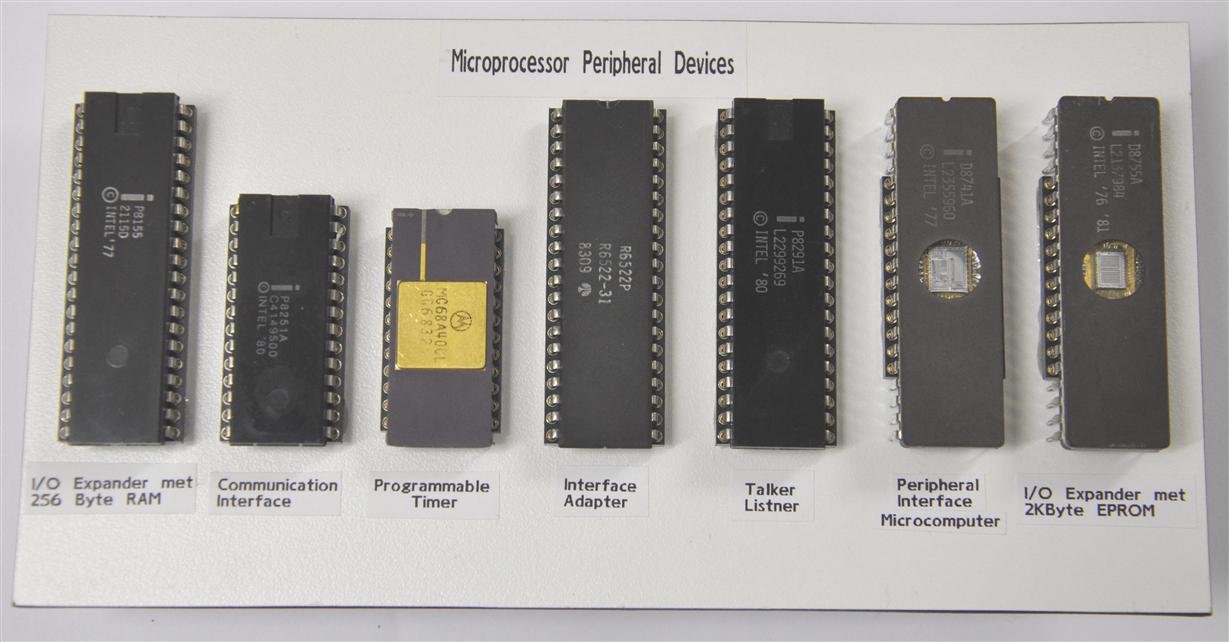
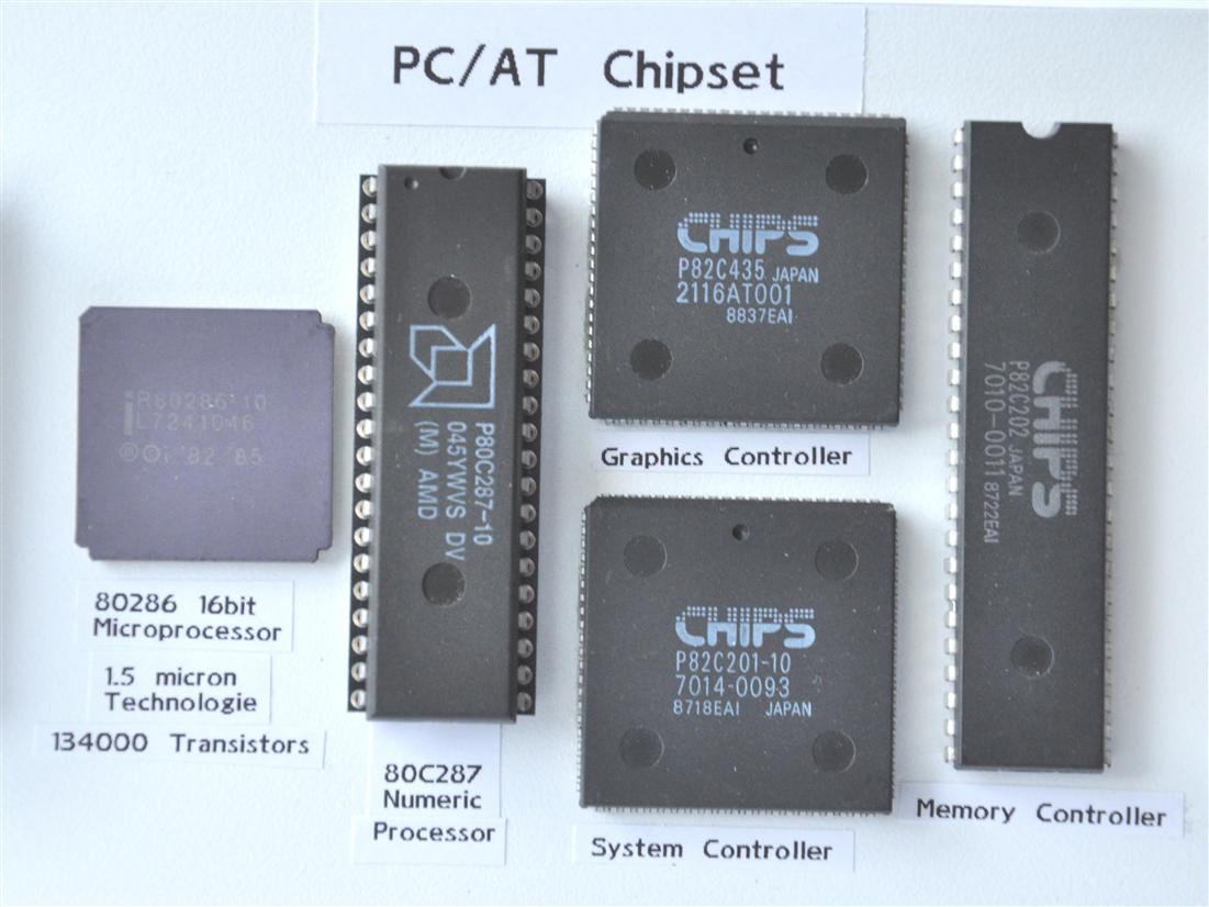
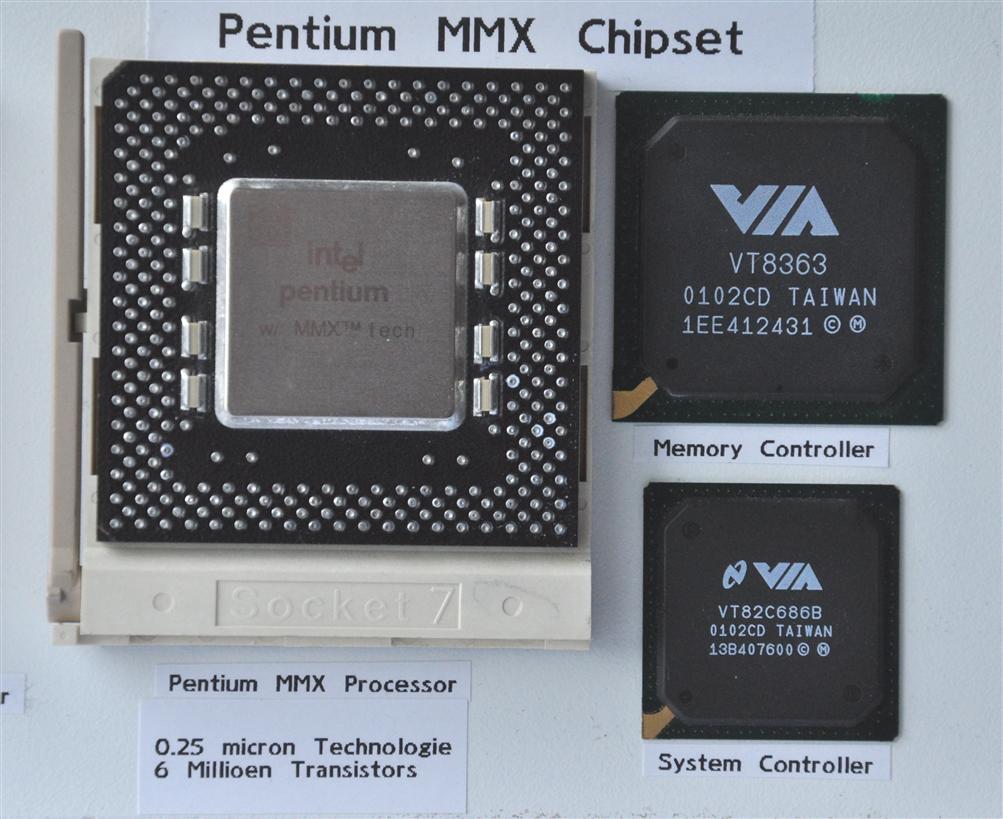
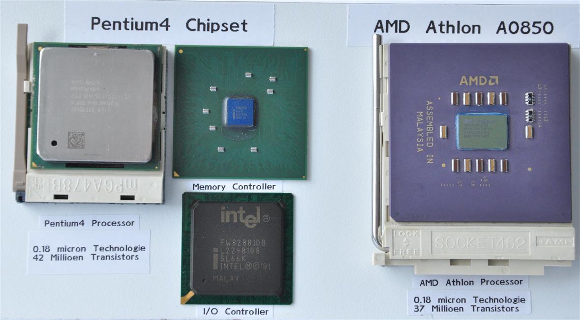
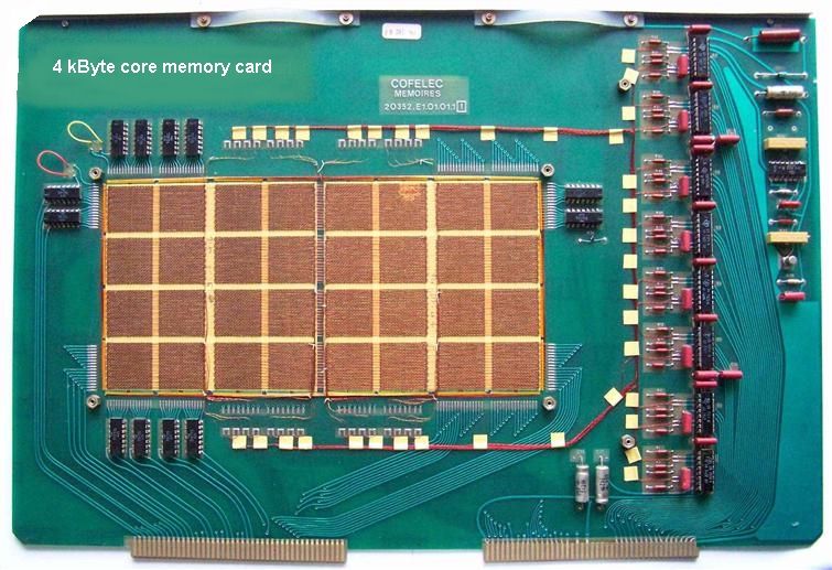
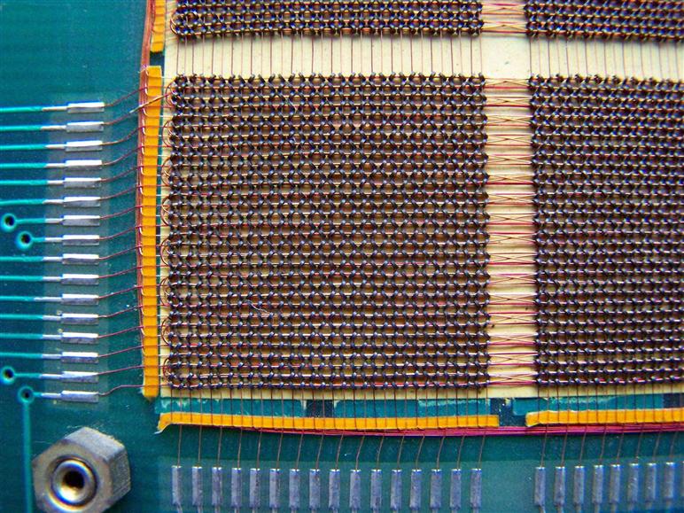
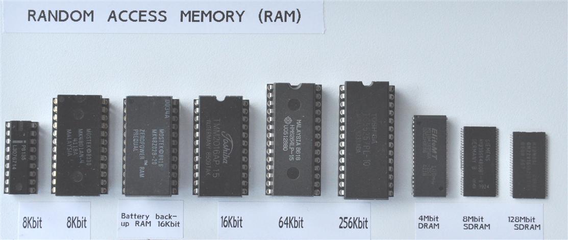
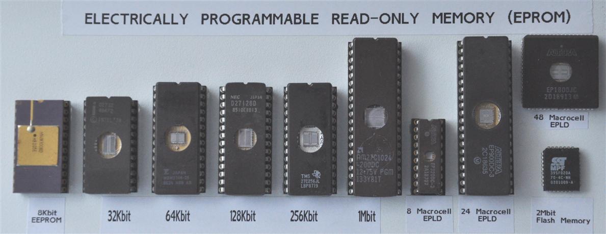
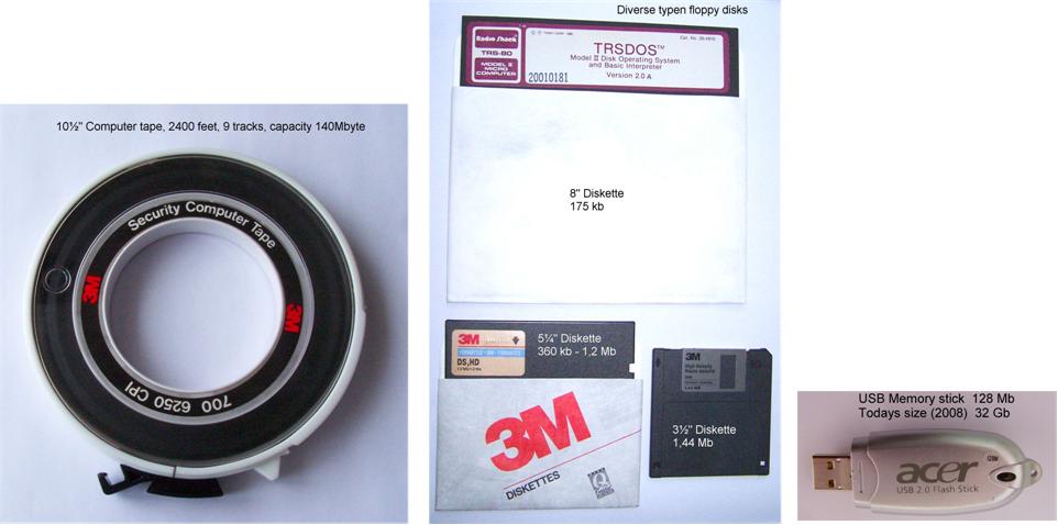
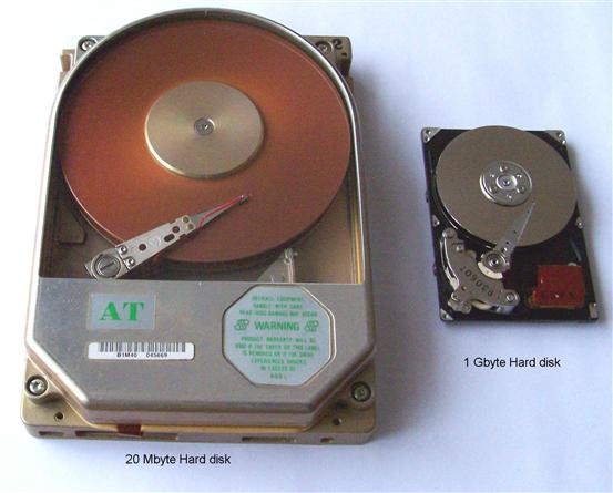